 | –≠–ª–µ–∫—Ç—Ä–æ–Ω–Ω—ã–π –∫–æ–º–ø–æ–Ω–µ–Ω—Ç: S07M-GS08 | –°–∫–∞—á–∞—Ç—å:  PDF PDF  ZIP ZIP |

S07B / 07D / 07G / 07J / 07M
Document Number 85733
Rev. 1.8, 13-Apr-05
Vishay Semiconductors
www.vishay.com
1
17249
Small Signal Fast Switching Diode, High Voltage
Features
∑ For surface mounted applications
∑ Low profile package
∑ Ideal for automated placement
∑ Glass passivated
∑ High temperature soldering:
260 ∞C/ 10 seconds at terminals
∑ Lead (Pb)-free component
∑ Component in accordance to RoHS 2002/95/EC
and WEEE 2002/96/EC
Mechanical Data
Case: JEDEC DO-219AB (SMF
Æ
) Plastic case
Polarity: Band denotes cathode end
Weight: approx. 15 mg
Packaging codes-options:
GS18 / 10 k per 13" reel (8 mm tape), 50 k/box
GS08 / 3 k per 7" reel (8 mm tape), 30 k/box
Parts Table
Part
Ordering code
Marking
Remarks
S07B
S07B-GS18 or S07B-GS08
SB
Tape and Reel
S07D
S07D-GS18 or S07D-GS08
SD
Tape and Reel
S07G
S07G-GS18 or S07G-GS08
SG
Tape and Reel
S07J
S07J-GS18 or S07J-GS08
SJ
Tape and Reel
S07M
S07M-GS18 or S07M-GS08
SM
Tape and Reel
e3

www.vishay.com
2
Document Number 85733
Rev. 1.8, 13-Apr-05
S07B / 07D / 07G / 07J / 07M
Vishay Semiconductors
Absolute Maximum Ratings
T
amb
= 25 ∞C, unless otherwise specified
1)
Averaged over any 20 ms period
Thermal Characteristics
T
amb
= 25 ∞C, unless otherwise specified
2)
Mounted on epoxy substrate with 3 x 3 mm CU pads (
40 µm thick)
Electrical Characteristics
T
amb
= 25 ∞C, unless otherwise specified
3)
Pulse test: 300
µ pulse width, 1 % duty cycle
Parameter
Test condition
Part
Symbol
Value
Unit
Maximum repetitive peak reverse voltage
S07B
V
RRM
100
V
S07D
V
RRM
200
V
S07G
V
RRM
400
V
S07J
V
RRM
600
V
S07M
V
RRM
1000
V
Maximum RMS voltage
S07B
V
RMS
70
V
S07D
V
RMS
140
V
S07G
V
RMS
280
V
S07J
V
RMS
420
V
S07M
V
RMS
700
V
Maximum DC blocking voltage
S07B
V
DC
100
V
S07D
V
DC
200
V
S07G
V
DC
400
V
S07J
V
DC
600
V
S07M
V
DC
1000
V
Maximum average forward rectified current
T
tp
= 75 ∞C
1)
I
F(AV)
1.5
A
T
A
= 65 ∞C
1)
I
F(AV)
0.7
A
Peak forward surge current 8.3 ms single
half sine-wave
T
L
= 25 ∞C
I
FSM
25
A
Parameter
Test condition
Symbol
Value
Unit
Thermal resistance junction to
ambient air
2)
R
thJA
180
K/W
Operating junction and storage
temperature range
T
J
, T
STG
- 55 to + 150
∞C
Parameter
Test condition
Symbol
Min
Typ.
Max
Unit
Maximum instantaneous
forward voltage
1.0 A
3)
V
F
1.1
V
Maximum DC reverse current at
rated DC blocking voltage
T
A
= 25 ∞C
I
R
10
µA
T
A
= 125 ∞C
I
R
50
µA
Reverse recovery time
I
F
= 0.5 A, I
R
= 1.0 A, I
rr
= 0.25 A
t
rr
1.8
µs
Typical capacitance at 4 V, MHz
C
j
4
pF
S07B / 07D / 07G / 07J / 07M
Document Number 85733
Rev. 1.8, 13-Apr-05
Vishay Semiconductors
www.vishay.com
3
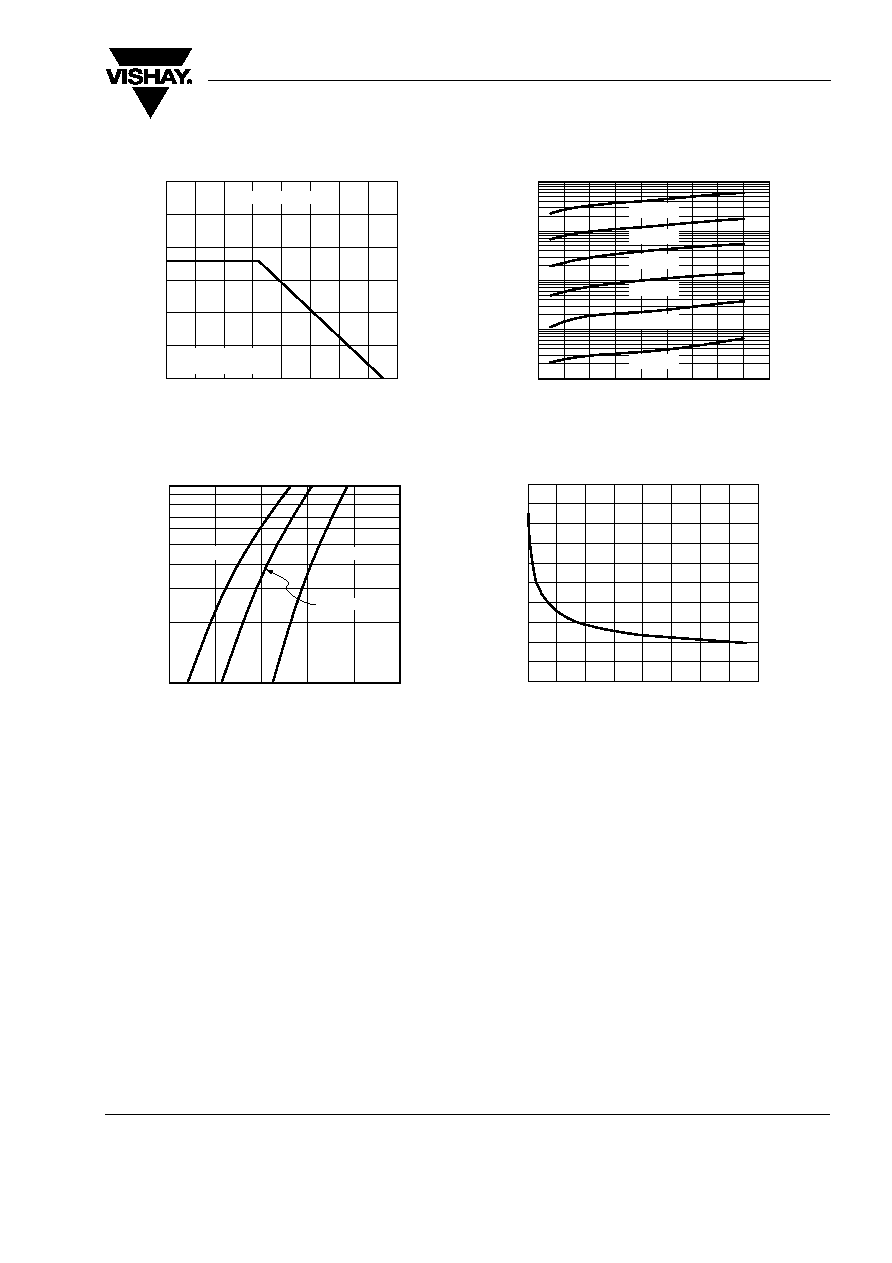
Typical Characteristics (Tamb = 25
∞C unless otherwise specified)
Figure 1. Forward Current Derating Curve
Figure 2. Typical Instantaneous Forward Characteristics
0
0.6
0.8
1.2
1.0
0
20
40
60
80
100
120
140
160
A
verage
Forward
Current
(A)
Ambient Temperature (
j
C)
0.4
0.2
Resistive or Inductive Load
3.0 x 3.0mm
40
µm
Thick Copper Pad Areas
17375
100
1000
600
700
800
900
1000
1100
Instantaneous
Forward
Current
(mA)
Instantaneous Forward Voltage (mV)
T
J
= 150
∞C
T
J
= 25
∞C
T
J
= 100
∞C
17376
Figure 3. Typical Instantaneous Reverse Characteristics
Figure 4. Capacitance vs. Reverse Voltage
Instantaneous
Reverse
Current
(
µ
A)
Instantaneous Reverse Voltage (V)
0
100
200
300
400
500
600
700
800
900
0.01
0.1
10
1
100
T
J
= 150
∞C
T
J
= 125
∞C
T
J
= 100
∞C
T
J
= 75
∞C
T
J
= 50
∞C
T
J
= 25
∞C
17377
V
R
(V)
C
(pF)
0
5
10
15
20
25
30
35
40
10
9
8
7
6
5
4
3
2
1
0
17378
www.vishay.com
4
Document Number 85733
Rev. 1.8, 13-Apr-05
S07B / 07D / 07G / 07J / 07M
Vishay Semiconductors
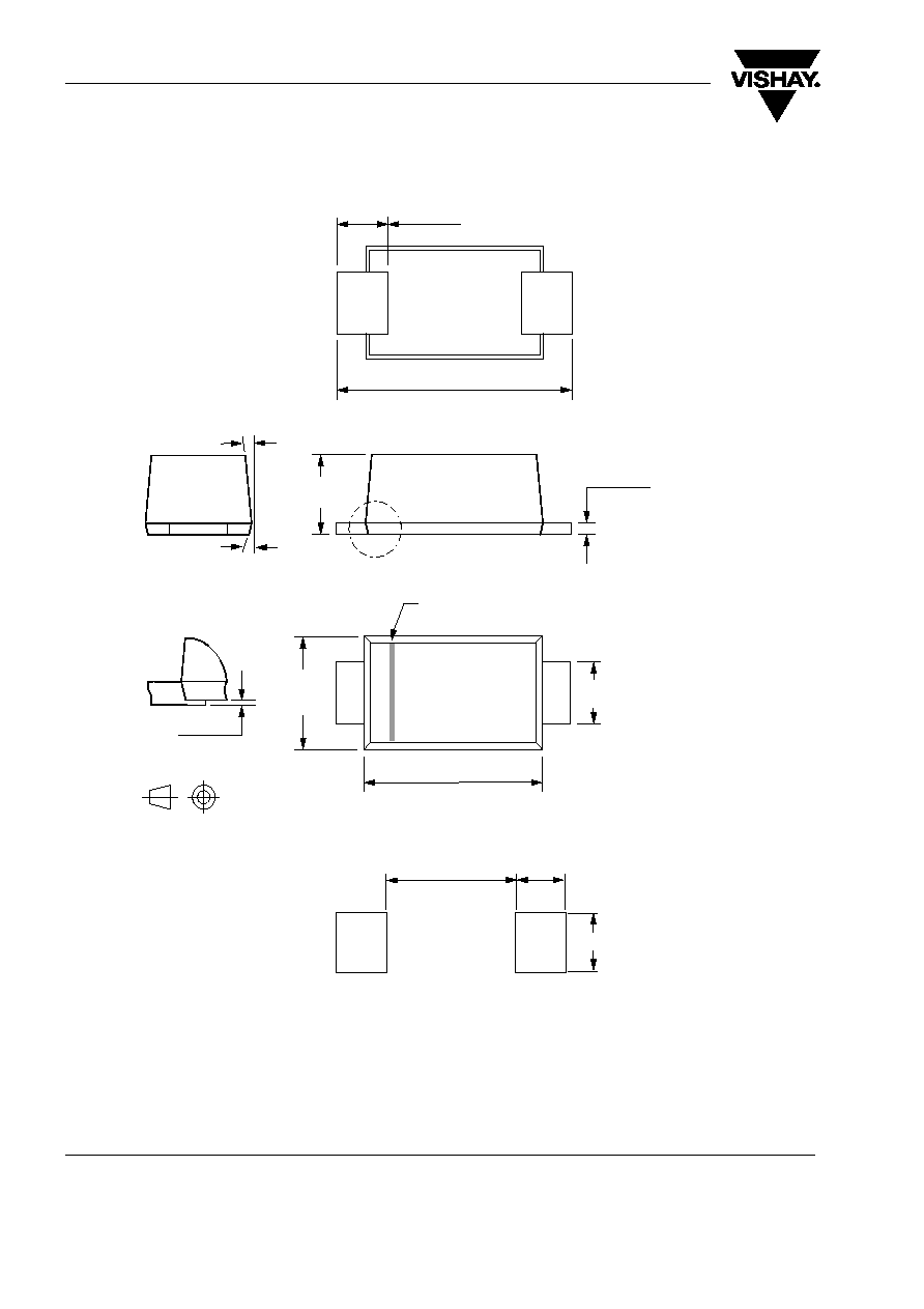
Package Dimensions in mm (Inches)
Top View
5
5
Z
Cathode Band
Detail
Z
enlarged
0.10 max
17247
0.85 (0.033)
0.35 (0.014)
3.9 (0.152)
3.5 (0.137)
0.99 (0.039)
0.97 (0.038)
0.16 (0.006)
1.9 (0.074)
1.7 (0.066)
1.2 (0.047)
0.8 (0.031)
2.9 (0.113)
2.7 (0.105)
ISO Method E
1.6 (0.062)
1.3 (0.051)
1.4 (0.055)
Mounting Pad Layout

S07B / 07D / 07G / 07J / 07M
Document Number 85733
Rev. 1.8, 13-Apr-05
Vishay Semiconductors
www.vishay.com
5
Blistertape for SMF
18513
PS