0.000 (0.00)
0.012 (0.30)
0.013 (0.35)
0.004 (0.10)
0.018 (0.45)
0.006 (0.15)
0.045 (1.15)
0.033 (0.85)
0.036 (0.91)
0.024 (0.61)
0.016 (0.40)
0.032 (0.80)
0.053 (1.35)
0.041 (1.05)
0.012 (0.30) REF
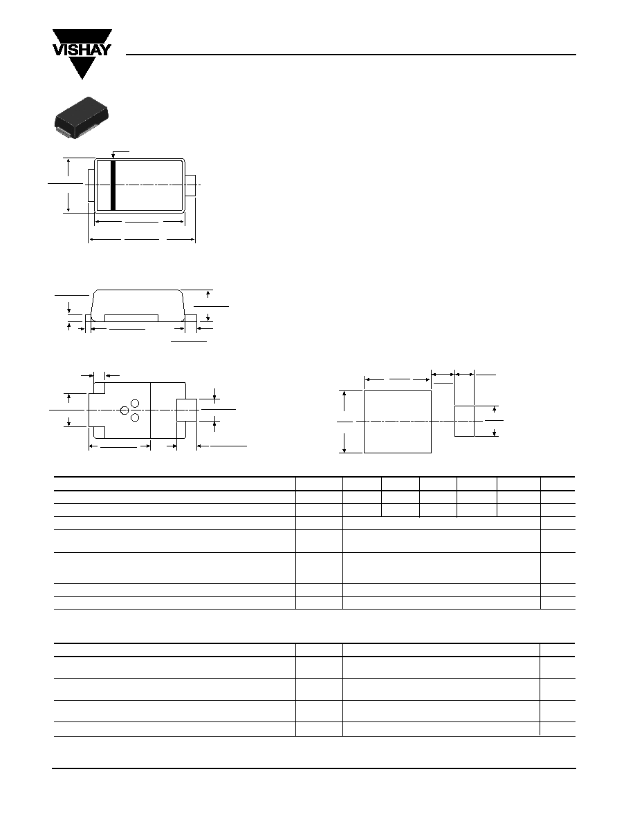
0.105
(2.67)
0.025
(0.635)
0.100
(2.54)
0.030
(0.762)
0.050
(1.27)
Cathode band
0.142 (3.61)
0.126 (3.19)
0.158 (4.00)
0.146 (3.70)
0.086 (2.18)
0.074 (1.88)
0.087 (2.20)
0.103 (2.60)
Dimensions in inches
and (millimeters)
Case Style SMP
Maximum Ratings & Thermal Characteristics
Ratings at 25∞C ambient temperature unless otherwise specified.
Parameter
Symbol
S1PA
S1PB
S1PD
S1PG
S1PJ
Unit
Device marking code
SA
SB
SD
SG
SJ
Maximum reverse voltage
V
RM
50
100
200
400
600
V
Maximum average forward rectified current Fig.1
I
F(AV)
1
A
Peak forward surge current 10ms single half sine-wave
superimposed on rated load
I
FSM
30
A
Typical thermal resistance
(1)
R
JA
105
R
JL
15
∞C/W
R
JC
20
Operating junction temperature
T
J
, 150
∞C
Storage temperature
T
STG
≠55 to +150
∞C
Electrical Characteristics
Ratings at 25∞C ambient temperature unless otherwise specified.
Parameter
Symbol
Value
Unit
Maximum instantaneous forward voltage
(2)
at I
F
=1A, T
J
=25∞C
V
F
1.1
V
at I
F
=1A, T
J
=125∞C
0.95
Maximum reverse current T
J
= 25∞C
1.0
µA
at rated VR
(2)
T
J
=125∞C
I
R
50
Typical reverse recovery time at
at I
F
= 0.5A, I
R
= 1.0A, I
rr
= 0.25A
trr
1.8
µs
Typical junction capacitance at 4.0V, 1MHz
C
J
6.0
pF
Notes: (1) Thermal resistance from junction to ambient and junction to lead mounted on P.C.B. with 5.0 x 5.0mm copper pad areas. R
JL
is measured at the ter-
minal of cathode band. R
JC
is measured at the top centre of the body
(2) Pulse test: 300µs pulse width, 1% duty cycle
Features
∑ Very low profile - typical height of 1.0mm
∑ Ideal for automated placement
∑ Glass passivated chip junction
∑ For use in rectification, power supply, home appliances
and telecommunication
∑ High temperature soldering:
260∞C maximum/10 seconds at terminals
∑ Meets MSL level 1 per J-STD-020C
Mechanical Data
Case: SMP
Terminals: Matte Tin plated (E3 Suffix) leads, solderable
per J-STD-002B and MIL-STD-750, Method 2026
Polarity: Color band denotes cathode end
Weight: 0.0009 oz., 0.024 g
Epoxy meets UL 94V-0 flammability rating
Mounting Pad Layout
S1PA thru S1PJ
Vishay Semiconductors
formerly General Semiconductor
High Current Density Surface Mount
Glass-Passivated Rectifiers
Reverse Voltage 50 to 600 V
Forward Current 1.0 A
Document Number 88917
www.vishay.com
23-Sep-04
1
New Product
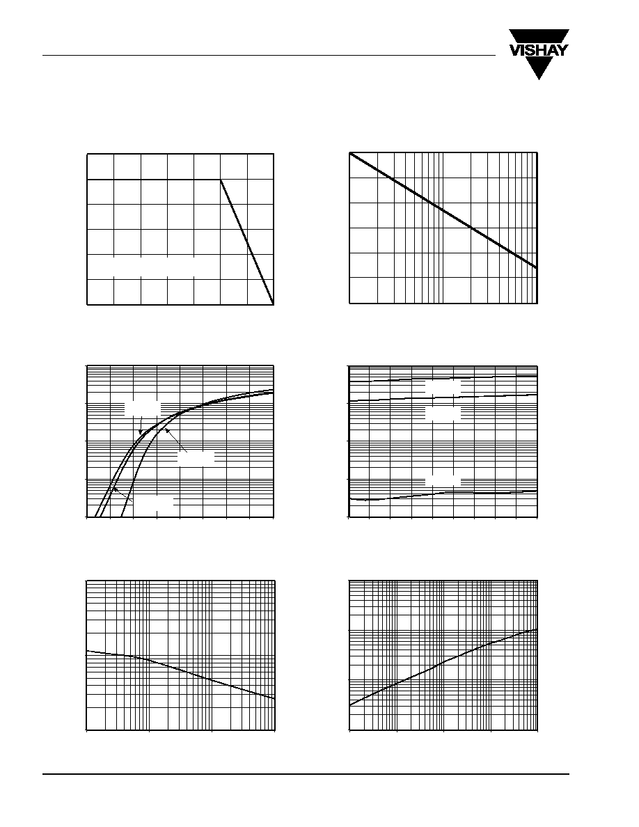
Fig. 2 ≠ Maximum Non-Repetitive Peak
Forward Surge Current
Peak Forward Surge Current (A)
Number of Cycles at 50 H
Z
0
1.2
80
90
100
110
120
130
140
150
Fig. 1 ≠ Maximum Forward Current
Derating Curve
A
verage Forward Rectified Current (A)
Lead Temperature (
∞
C)
0.4
0.6
0.8
1.2
1.4
Instantaneous Forward Voltage (V)
Fig. 3 ≠ Typical Instantaneous
Forward Characteristics
0.01
1
10
100
Fig. 4 ≠ Typical Reverse Leakage
Characteristics
Instantaneous Reverse Current (
µ
A)
Percent of Rated Peak Reverse Voltage (%)
0.8
1.0
0.2
0.4
0.6
20
40
60
80
100
0.1
1
10
100
0.1
10
1
100
Instantaneous Forward Current (A)
Reverse Voltage (V)
Junction Capacitance (pF)
1
10
100
Fig. 5 ≠ Typical Junction Capacitance
t, Pulse Duration (sec.)
T
ransient
Thermal Impedance (
∞
C/W)
Fig. 6 ≠ Typical Transient Thermal
Impedance
1
10
100
10
20
30
0
0.1
1
10
100
1
100
1000
0.1
1000
10
30
50
70
90
0.01
05
15
25
1.8
2.0
1.0
1.6
0.01
T
L
measured
at the cathode band terminal
T
J
= 150
∞
C
T
J
= 25
∞
C
T
J
= 125
∞
C
T
J
= 25
∞
C
T
J
= 125
∞
C
T
J
= 150
∞
C
S1PA thru S1PJ
Vishay Semiconductors
formerly General Semiconductor
Ratings and
Characteristic Curves
(T
A
= 25∞C unless otherwise noted)
www.vishay.com
Document Number 88917
2
23-Sep-04