 | –≠–ª–µ–∫—Ç—Ä–æ–Ω–Ω—ã–π –∫–æ–º–ø–æ–Ω–µ–Ω—Ç: S503TX | –°–∫–∞—á–∞—Ç—å:  PDF PDF  ZIP ZIP |
VISHAY
S503TX/S503TXR/S503TXRW
Document Number 85078
Rev. 1.2, 30-Aug-04
Vishay Semiconductors
www.vishay.com
1
19216
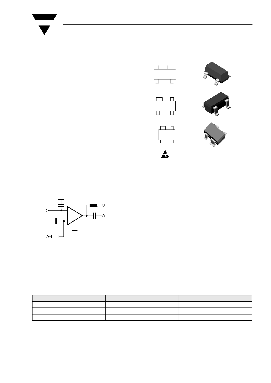
SOT-143
SOT-143R
SOT-343R
1
2
4
3
2
1
3
4
Electrostatic sensitive device.
Observe precautions for handling.
1
2
4
3
MOSMIC
Æ
for TV-Tuner Prestage with 5 V Supply Voltage
Comments
MOSMIC - MOS Monolithic Integrated Circuit
Features
∑ Easy Gate 1 switch-off with PNP switching transis-
tors inside PLL
∑ High AGC-range with less steep slope
∑ Integrated gate protection diodes
∑ Low noise figure
∑ High gain, very high forward transadmittance
(40 mS typ.)
∑ Improved cross modulation at gain reduction
∑ SMD package
Applications
Low noise gain controlled input stages in UHF-and
VHF- tuner with 5 V supply voltage.
Typical Application
Mechanical Data
Typ: S503TX
Case: SOT-143 Plastic case
Weight: approx. 8.0 mg
Pinning: 1 = Source, 2 = Drain,
3 = Gate 2, 4 = Gate 1
Typ: S503TXR
Case: SOT-143R Plastic case
Weight: approx. 8.0 mg
Pinning: 1 = Source, 2 = Drain,
3 = Gate 2, 4 = Gate 1
Typ: S503TXRW
Case: SOT-343R Plastic case
Weight: approx. 6.0 mg
Pinning: 1 = Source, 2 = Drain,
3 = Gate 2, 4 = Gate 1
Parts Table
G2
G1
RF in
S
D
V
DD
(V
DS
)
C block
RFC
RF out
13650
C block
C block
RG1
V
GG
(V
RG1
)
AGC
Part
Marking
Package
S503TX
X03
SOT-143
S503TXR
X8R
SOT-143R
S503TXRW
WX8
SOT-343R

www.vishay.com
2
Document Number 85078
Rev. 1.2, 30-Aug-04
VISHAY
S503TX/S503TXR/S503TXRW
Vishay Semiconductors
Absolute Maximum Ratings
T
amb
= 25 ∞C, unless otherwise specified
Maximum Thermal Resistance
1)
on glass fibre printed board (25 x 20 x 1.5) mm
3
plated with 35
µm Cu
Electrical DC Characteristics
T
amb
= 25 ∞C, unless otherwise specified
Remark on improving intermodulation behavior:
By setting R
G1
smaller than 56 k
, typical value of I
DSO
will raise and improved intermodulation behavior will be performed.
Electrical AC Characteristics
T
amb
= 25 ∞C, unless otherwise specified
V
DS
= 5 V, V
G2S
= 4 V, I
D
= 13 mA, f = 1 MHz
Parameter
Test condition
Symbol
Value
Unit
Drain - source voltage
V
DS
8
V
Drain current
I
D
30
mA
Gate 1/Gate 2 - source peak
current
± I
G1/G2SM
10
mA
Gate 1 - source voltage
+ V
G1S
6
V
- V
G1S
1.5
V
Gate 2 - source voltage
± V
G2SM
6
V
Total power dissipation
T
amb
60 ∞C
P
tot
200
mW
Channel temperature
T
Ch
150
∞C
Storage temperature range
T
stg
- 55 to + 150
∞C
Parameter
Test condition
Symbol
Value
Unit
Channel ambient
1)
R
thChA
450
K/W
Parameter
Test condition
Symbol
Min
Typ.
Max
Unit
Drain - source breakdown
voltage
I
D
= 10
µA, V
G1S
= V
G2S
= 0
V
(BR)DSS
12
V
Gate 1 - source breakdown
voltage
± I
G1S
= 10 mA, V
G2S
= V
DS
= 0 ± V
(BR)G1SS
7
10
V
Gate 2 - source breakdown
voltage
± I
G2S
= 10 mA, V
G1S
= V
DS
= 0 ± V
(BR)G2SS
7
10
V
Gate 1 - source leakage current + V
G1S
= 5 V, V
G2S
= V
DS
= 0
+ I
G1SS
20
nA
Gate 2 - source leakage current ± V
G2S
= 5 V, V
G1S
= V
DS
= 0
± I
G2SS
20
nA
Drain - source operating current V
DS
= V
RG1
= 5 V, V
G2S
= 4 V,
R
G1
= 56 k
I
DSO
10
15
20
mA
Gate 1 - source cut-off voltage
V
DS
= 5 V, V
G2S
= 4, I
D
= 20
µA
V
G1S(OFF)
0.3
1.3
V
Gate 2 - source cut-off voltage
V
DS
= V
RG1
= 5 V, R
G1
= 56 k
,
I
D
= 20
µA
V
G2S(OFF)
0.8
1.0
1.4
V
Parameter
Test condition
Symbol
Min
Typ.
Max
Unit
Forward transadmittance
|y
21s
|
35
40
50
mS
Gate 1 input capacitance
C
issg1
2.3
2.8
pF
Feedback capacitance
C
rss
30
40
fF
Output capacitance
C
oss
1.4
pF

VISHAY
S503TX/S503TXR/S503TXRW
Document Number 85078
Rev. 1.2, 30-Aug-04
Vishay Semiconductors
www.vishay.com
3
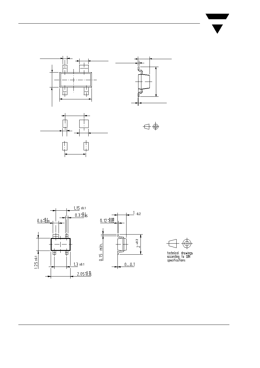
Package Dimensions in mm
Power gain
G
S
= 2 mS, G
L
= 0.5 mS,
f = 200 MHz
G
ps
30
dB
G
S
= 3,3 mS, G
L
= 1 mS,
f = 800 MHz
G
ps
18
24
dB
AGC range
V
DS
= 5 V, V
G2S
= 1 to 4 V,
f = 800 MHz
G
ps
40
45
dB
Noise figure
G
S
= 2 mS, G
L
= 0.5 mS,
f = 200 MHz
F
1
dB
G
S
= 3.3 mS, G
L
= 1 mS,
f = 800 MHz
F
1.3
dB
Cross modulation
Input level for k = 1 % @ 0 dB
AGC f
w
= 50 MHz,
f
unw
= 60 MHz
X
mod
90
dB
µV
Input level for k = 1 % @ 40 dB
AGC f
w
= 50 MHz,
f
unw
= 60 MHz
X
mod
100
105
dB
µV
Parameter
Test condition
Symbol
Min
Typ.
Max
Unit
96 12239
www.vishay.com
4
Document Number 85078
Rev. 1.2, 30-Aug-04
VISHAY
S503TX/S503TXR/S503TXRW
Vishay Semiconductors
Package Dimensions in mm
Package Dimensions in mm
Mounting Pad Layout
96 12240
0.50(0.020)
0.35 (0.014)
1.8 (0.070)
1.6 (0.062)
0.9 (0.035)
0.75 (0.029)
1.4
(0.055)
1.2
(0.047)
2.0 (0.078)
1.8 (0.070)
3.0 (0.117)
2.8 (0.109)
0.15 (0.006)
0.08 (0.003)
1.1 (0.043)
0.9 (0.035)
0...0.1 (0...0.004)
2.6
(0.101)
2.4
(0.094)
ISO Method E
0.65 (0.025)
1.17 (0.046)
96 12238

VISHAY
S503TX/S503TXR/S503TXRW
Document Number 85078
Rev. 1.2, 30-Aug-04
Vishay Semiconductors
www.vishay.com
5
Ozone Depleting Substances Policy Statement
It is the policy of Vishay Semiconductor GmbH to
1. Meet all present and future national and international statutory requirements.
2. Regularly and continuously improve the performance of our products, processes, distribution and
operatingsystems with respect to their impact on the health and safety of our employees and the public, as
well as their impact on the environment.
It is particular concern to control or eliminate releases of those substances into the atmosphere which are
known as ozone depleting substances (ODSs).
The Montreal Protocol (1987) and its London Amendments (1990) intend to severely restrict the use of ODSs
and forbid their use within the next ten years. Various national and international initiatives are pressing for an
earlier ban on these substances.
Vishay Semiconductor GmbH has been able to use its policy of continuous improvements to eliminate the
use of ODSs listed in the following documents.
1. Annex A, B and list of transitional substances of the Montreal Protocol and the London Amendments
respectively
2. Class I and II ozone depleting substances in the Clean Air Act Amendments of 1990 by the Environmental
Protection Agency (EPA) in the USA
3. Council Decision 88/540/EEC and 91/690/EEC Annex A, B and C (transitional substances) respectively.
Vishay Semiconductor GmbH can certify that our semiconductors are not manufactured with ozone depleting
substances and do not contain such substances.
We reserve the right to make changes to improve technical design
and may do so without further notice.
Parameters can vary in different applications. All operating parameters must be validated for each
customer application by the customer. Should the buyer use Vishay Semiconductors products for any
unintended or unauthorized application, the buyer shall indemnify Vishay Semiconductors against all
claims, costs, damages, and expenses, arising out of, directly or indirectly, any claim of personal
damage, injury or death associated with such unintended or unauthorized use.
Vishay Semiconductor GmbH, P.O.B. 3535, D-74025 Heilbronn, Germany
Telephone: 49 (0)7131 67 2831, Fax number: 49 (0)7131 67 2423