 | –≠–ª–µ–∫—Ç—Ä–æ–Ω–Ω—ã–π –∫–æ–º–ø–æ–Ω–µ–Ω—Ç: SC-75A | –°–∫–∞—á–∞—Ç—å:  PDF PDF  ZIP ZIP |
Si1013R/X
Vishay Siliconix
New Product
Document Number: 71167
S-02464--Rev. A, 25-Oct-00
www.vishay.com
1
P-Channel 1.8-V (G-S) MOSFET
PRODUCT SUMMARY
V
DS
(V)
r
DS(on)
(
W
)
I
D
(mA)
1.2 @ V
GS
= ≠4.5 V
≠350
≠20
1.6 @ V
GS
= ≠2.5 V
≠300
2.7 @ V
GS
= ≠1.8 V
≠150
FEATURES
BENEFITS
APPLICATIONS
D
High-Side Switching
D
Low On-Resistance: 1.2
W
D
Low Threshold: 0.8 V (typ)
D
Fast Swtiching Speed: 14 ns
D
1.8-V Operation
D
Gate-Source ESD Protection
D
Ease in Driving Switches
D
Low Offset (Error) Voltage
D
Low-Voltage Operation
D
High-Speed Circuits
D
Low Battery Voltage Operation
D
Drivers: Relays, Solenoids, Lamps,
Hammers, Displays, Memories
D
Battery Operated Systems
D
Power Supply Converter Circuits
D
Load/Power Switching Cell Phones, Pagers
SC-75A or SC-89
Top View
2
1
S
D
G
3
Ordering Information:
SC-75A (SOT≠ 416):
Si1013R≠Marking Code : D
SC-89 (SOT≠ 490):
Si1013X≠Marking Code: B
ABSOLUTE MAXIMUM RATINGS (T
A
= 25_C UNLESS OTHERWISE NOTED)
Parameter
Symbol
5 secs
Steady State
Unit
Drain-Source Voltage
V
DS
≠20
Gate-Source Voltage
V
GS
"
6
V
_
T
A
= 25
_
C
≠400
≠350
Continuous Drain Current
(T
J
= 150
_
C)
b
T
A
= 85
_
C
I
D
≠300
≠275
Pulsed Drain Current
a
I
DM
≠1000
mA
Continuous Source Current (diode conduction)
b
I
S
≠275
≠250
T
A
= 25
_
C
175
150
Maximum Power Dissipation
b
for SC-75
T
A
= 85
_
C
90
80
T
A
= 25
_
C
P
D
275
250
mW
Maximum Power Dissipation
b
for SC-89
T
A
= 85
_
C
160
140
Operating Junction and Storage Temperature Range
T
J
, T
stg
≠55 to 150
_
C
Gate-Source ESD Rating (HBM, Method 3015)
ESD
2000
V
Notes
a.
Pulse width limited by maximum junction temperature.
b.
Surface Mounted on FR4 Board.
Si1013R/X
Vishay Siliconix
New Product
www.vishay.com
2
Document Number: 71167
S-02464--Rev. A, 25-Oct-00
SPECIFICATIONS (T
A
= 25_C UNLESS OTHERWISE NOTED)
Parameter
Symbol
Test Condition
Min
Typ
Max
Unit
Static
Gate Threshold Voltage
V
GS(th)
V
DS
= V
GS
, I
D
= ≠250
m
A
≠0.45
V
Gate-Body Leakage
I
GSS
V
DS
= 0 V, V
GS
=
"
4.5
V
"
1
"
2
m
A
V
DS
= ≠16 V, V
GS
= 0 V
≠0.3
≠100
nA
Zero Gate Voltage Drain Current
I
DSS
V
DS
= ≠16 V, V
GS
= 0 V, T
J
= 85
_
C
≠5
m
A
On-State Drain Current
a
I
D(on)
V
DS
= ≠5 V, V
GS
= ≠4.5 V
≠700
mA
V
GS
= ≠4.5 V, I
D
= ≠350 mA
0.8
1.2
Drain-Source On-State Resistance
a
r
DS(on)
V
GS
= ≠2.5 V, I
D
= ≠300 m A
1.2
1.6
W
DS(on)
V
GS
= ≠1.8 V, I
D
= ≠150 m A
1.8
2.7
Forward Transconductance
a
g
fs
V
DS
= ≠10
V, I
D
= ≠250 mA
0.4
S
Diode Forward Voltage
a
V
SD
I
S
= ≠150 mA, V
GS
= 0 V
≠0.8
≠1.2
V
Dynamic
b
Total Gate Charge
Q
g
1500
Gate-Source Charge
Q
gs
V
DS
= ≠10 V,
V
GS
= ≠4.5 V, I
D
= ≠250 mA
150
pC
Gate-Drain Charge
Q
gd
450
Turn-On Delay Time
t
d(on)
5
Rise Time
t
r
V
DD
= ≠10 V, R
L
= 47
W
9
Turn-Off Delay Time
t
d(off)
V
DD
= ≠10 V, R
L
= 47
W
I
D
^
≠200 mA, V
GEN
= ≠4.5 V, R
G
= 10
W
35
ns
Fall Time
t
f
11
Notes
a.
Pulse test; pulse width
v
300
m
s, duty cycle
v
2%.
b.
Guaranteed by design, not subject to production testing.
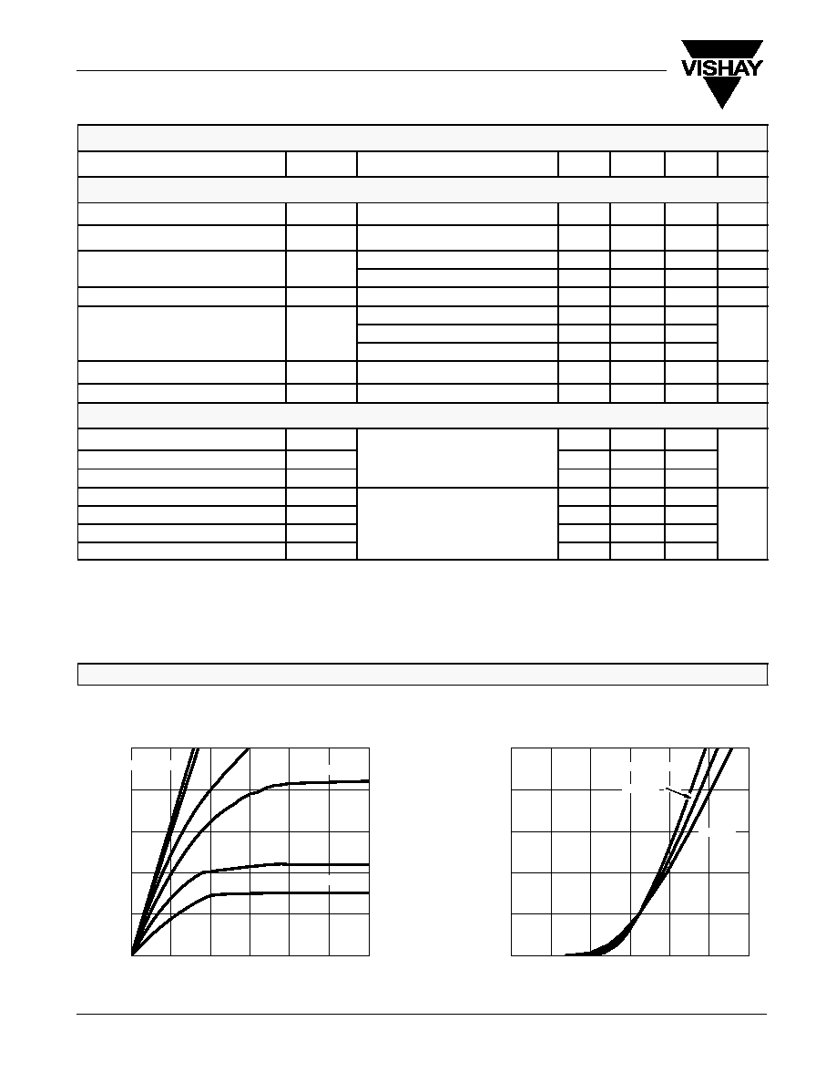
TYPICAL CHARACTERISTICS (T
A
= 25_C UNLESS NOTED)
For the following graphs, p-channel negative polarities for all voltage and current values are represented as positive values.
0
200
400
600
800
1000
0.0
0.5
1.0
1.5
2.0
2.5
3.0
0.0
0.2
0.4
0.6
0.8
1.0
0.0
0.5
1.0
1.5
2.0
2.5
3.0
V
GS
= 5 thru 3 V
T
J
= ≠55
_
C
125
_
C
2 V
25
_
C
Output Characteristics
Transfer Characteristics
V
DS
≠ Drain-to-Source Voltage (V)
≠
Drain Current (A)
I
D
V
GS
≠ Gate-to-Source Voltage (V)
≠
Drain Current (mA)
I
D
1.8 V
2.5 V
Si1013R/X
Vishay Siliconix
New Product
Document Number: 71167
S-02464--Rev. A, 25-Oct-00
www.vishay.com
3
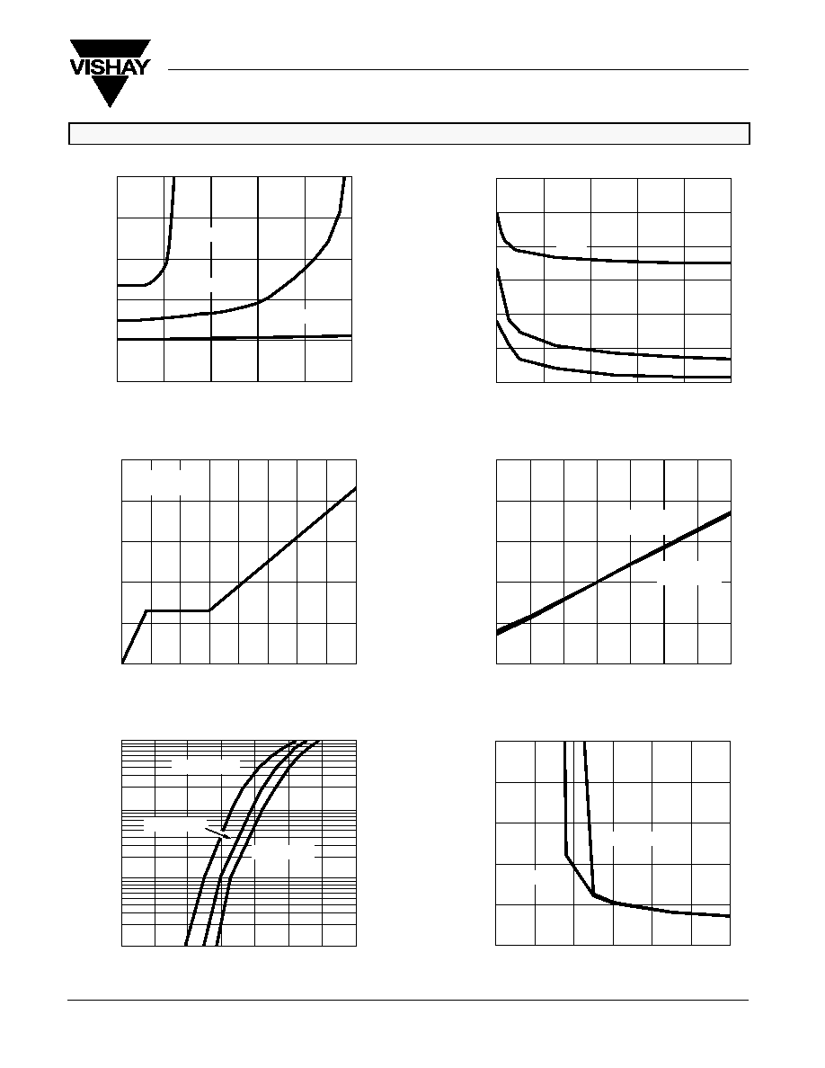
TYPICAL CHARACTERISTICS (T
A
= 25_C UNLESS NOTED)
0.0
0.2
0.4
0.6
0.8
1.0
1.2
1.4
≠
On-Resistance (
r
DS(on)
W
)
0
20
40
60
80
100
120
0
4
8
12
16
20
0.6
0.8
1.0
1.2
1.4
1.6
≠50
≠25
0
25
50
75
100
125
0
1
2
3
4
5
0.0
0.2
0.4
0.6
0.8
1.0
1.2
1.4
1.6
0.0
0.8
1.6
2.4
3.2
4.0
0
200
400
600
800
1000
V
DS
≠ Drain-to-Source Voltage (V)
C
rss
C
oss
C
iss
V
DS
= 10 V
I
D
= 250 mA
I
D
≠ Drain Current (mA)
V
GS
= 4.5 V
I
D
= 350 mA
V
GS
= 1.8 V
Gate Charge
On-Resistance vs. Drain Current
≠
Gate-to-Source V
oltage (V)
Q
g
≠ Total Gate Charge (nC)
C
≠
Capacitance (pF)
V
GS
Capacitance
On-Resistance vs. Junction Temperature
T
J
≠ Junction Temperature (
_
C)
(Normalized)
≠
On-Resistance (
r
DS(on)
W
)
0
1
2
3
4
5
0
1
2
3
4
5
6
I
D
= 350 mA
1000
1
Source-Drain Diode Forward Voltage
On-Resistance vs. Gate-to-Source Voltage
≠
On-Resistance (
r
DS(on)
W
)
V
SD
≠ Source-to-Drain Voltage (V)
V
GS
≠ Gate-to-Source Voltage (V)
V
GS
= 4.5 V
I
D
= 200 mA
V
GS
= 2.5 V
V
GS
= 1.8 V
I
D
= 150 mA
T
J
= 125
_
C
T
J
= 25
_
C
T
J
= ≠55
_
C
10
100
I
S
≠
Source Current (mA)
Si1013R/X
Vishay Siliconix
New Product
www.vishay.com
4
Document Number: 71167
S-02464--Rev. A, 25-Oct-00
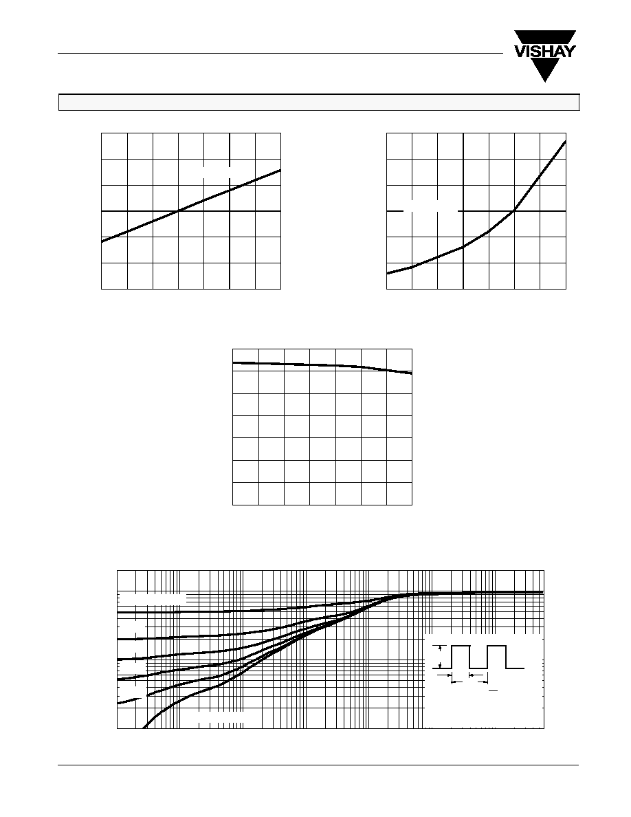
TYPICAL CHARACTERISTICS (T
A
= 25_C UNLESS NOTED)
≠0.3
≠0.2
≠0.1
≠0.0
0.1
0.2
0.3
≠50
≠25
0
25
50
75
100
125
I
D
= 0.25 mA
Threshold Voltage Variance vs. Temperature
V
ariance (V)
V
GS(th)
T
J
≠ Temperature (
_
C)
0.0
0.5
1.0
1.5
2.0
2.5
3.0
≠50
≠25
0
25
50
75
100
125
I
GSS
vs. Temperature
T
J
≠ Temperature (
_
C)
I
GS
S
≠
(
m
A)
0
1
2
3
4
5
6
7
≠50
≠25
0
25
50
75
100
125
BV
GSS
vs. Temperature
T
J
≠ Temperature (
_
C)
V
GS
= 4.5 V
BV
GS
S
≠
Gate-to-Source Breakdown V
oltage (V)
10
≠3
10
≠2
1
10
600
10
≠1
10
≠4
100
2
1
0.1
0.01
0.2
0.1
0.05
0.02
Single Pulse
Duty Cycle = 0.5
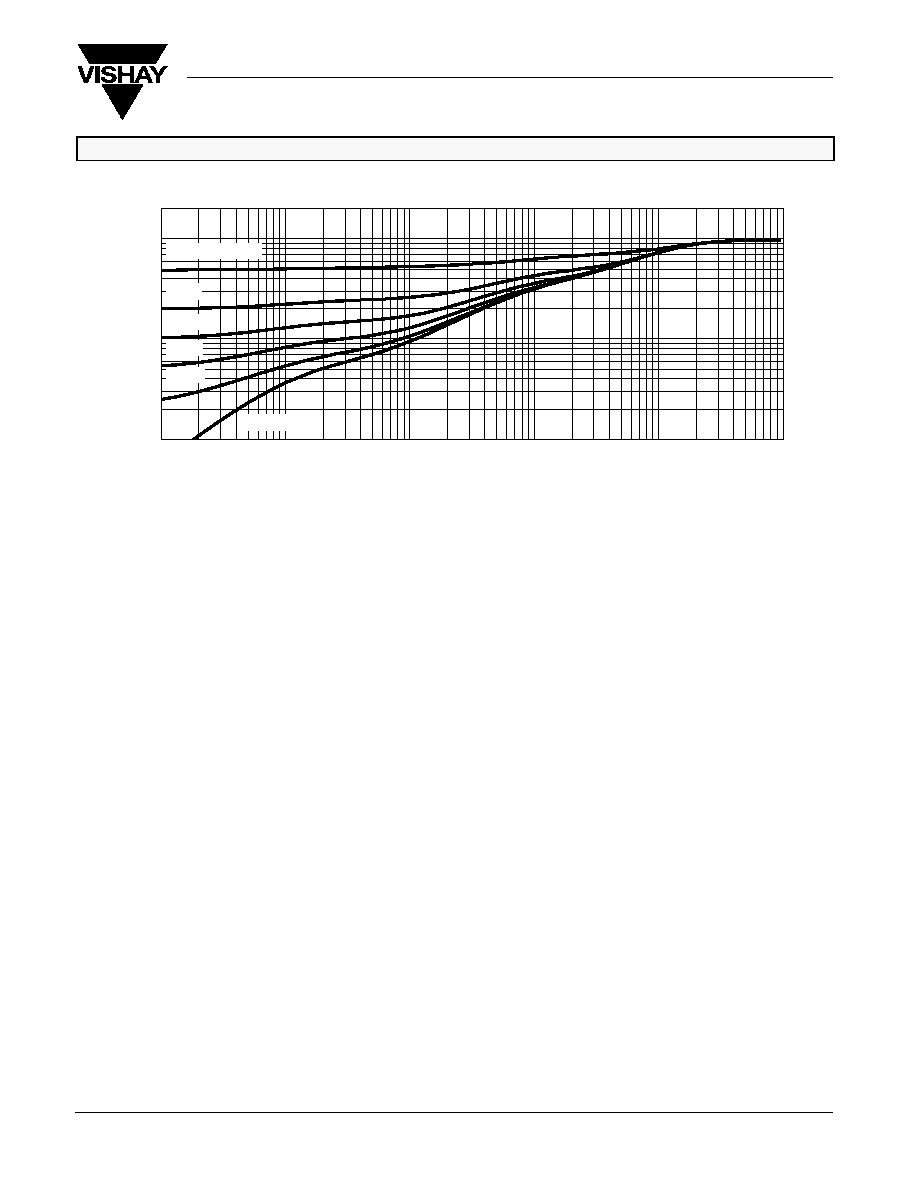
Normalized Thermal Transient Impedance, Junction-to-Ambient (SC-75A)
Square Wave Pulse Duration (sec)
Normalized Ef
fective
T
ransient
Thermal Impedance
1. Duty Cycle, D =
2. Per Unit Base = R
thJA
=833
_
C/W
3. T
JM
≠ T
A
= P
DM
Z
thJA
(t)
t
1
t
2
t
1
t
2
Notes:
4. Surface Mounted
P
DM
Si1013R/X
Vishay Siliconix
New Product
Document Number: 71167
S-02464--Rev. A, 25-Oct-00
www.vishay.com
5
TYPICAL CHARACTERISTICS (T
A
= 25_C UNLESS NOTED)
10
≠3
10
≠2
1
10
10
≠1
10
≠4
2
1
0.1
0.01
0.2
0.1
0.05
0.02
Single Pulse
Duty Cycle = 0.5
Normalized Thermal Transient Impedance, Junction-to-Foot
Square Wave Pulse Duration (sec)
Normalized Ef
fective
T
ransient
Thermal Impedance