 | –≠–ª–µ–∫—Ç—Ä–æ–Ω–Ω—ã–π –∫–æ–º–ø–æ–Ω–µ–Ω—Ç: SFH601-3 | –°–∫–∞—á–∞—Ç—å:  PDF PDF  ZIP ZIP |
VISHAY
SFH601
Document Number 83663
Rev. 1.4, 26-Oct-04
Vishay Semiconductors
www.vishay.com
1
i179004
i179004
1
2
3
6
5
4
B
C
E
A
C
NC
Pb
Pb-free
e3
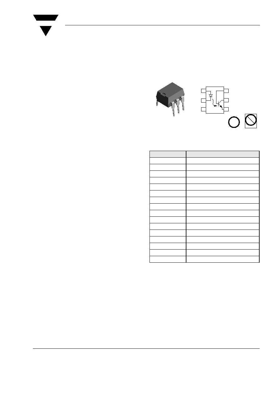
Optocoupler, Phototransistor Output, With Base Connection
Features
∑ Isolation Test Voltage (1.0 s), 5300 V
RMS
∑ V
CEsat
0.25 (
0.4) V, I
F
= 10 mA, I
C
= 2.5 mA
∑ Built to conform to VDE Requirements
∑ Highest Quality Premium Device
∑ Long Term Stability
∑ Storage Temperature, - 55 ∞ to + 150 ∞C
∑ Lead-free component
∑ Component in accordance to RoHS 2002/95/EC
and WEEE 2002/96/EC
Agency Approvals
∑ UL1577, File No. E52744 System Code H or J,
Double Protection
∑ DIN EN 60747-5-2 (VDE0884)
DIN EN 60747-5-5 pending
Available with Option 1
∑ CSA 93751
∑ BSI IEC60950 IEC60065
Description
The SFH601 is an optocoupler with a Gallium Ars-
enide LED emitter which is optically coupled with a sil-
icon planar phototransistor detector. The component
is packaged in a plastic plug-in case 20 AB DIN
41866.
The coupler transmits signals between two electri-
cally isolated circuits.
Order Information
For additional information on the available options refer to
Option Information.
Part
Remarks
SFH601-1
CTR 40 - 80 %, DIP-6
SFH601-2
CTR 63 - 125 %, DIP-6
SFH601-3
CTR 100 - 200 %, DIP-6
SFH601-4
CTR 160 - 320 %, DIP-6
SFH601-1X006
CTR 40 - 80 %, DIP-6 400 mil (option 6)
SFH601-1X007
CTR 40 - 80 %, SMD-6 (option 7)
SFH601-1X009
CTR 40 - 80 %, SMD-6 (option 9)
SFH601-2X006
CTR 63 - 125 %, DIP-6 400 mil (option 6)
SFH601-2X007
CTR 63 - 125 %, SMD-6 (option 7)
SFH601-2X009
CTR 63 - 125 %, SMD-6 (option 9)
SFH601-3X006
CTR 100 - 200 %, DIP-6 400 mil (option 6)
SFH601-3X007
CTR 100 - 200 %, SMD-6 (option 7)
SFH601-3X009
CTR 100 - 200 %, SMD-6 (option 9)
SFH601-4X006
CTR 160 - 320 %, DIP-6 400 mil (option 6)
SFH601-4X007
CTR 160 - 320 %, SMD-6 (option 7)
SFH601-4X009
CTR 160 - 320 %, SMD-6 (option 9)
www.vishay.com
2
Document Number 83663
Rev. 1.4, 26-Oct-04
VISHAY
SFH601
Vishay Semiconductors
Absolute Maximum Ratings
T
amb
= 25 ∞C, unless otherwise specified
Stresses in excess of the absolute Maximum Ratings can cause permanent damage to the device. Functional operation of the device is
not implied at these or any other conditions in excess of those given in the operational sections of this document. Exposure to absolute
Maximum Rating for extended periods of the time can adversely affect reliability.
Input
Output
Coupler
1)
between emitter and detector referred to climate DIN 40046, part 2, Nov. 74
2)
index per DIN IEC 60112/VDE0303, part 1
Parameter
Test condition
Symbol
Value
Unit
Reverse voltage
V
R
6.0
V
DC forward current
I
F
60
mA
Surge forward current
t =10
µs
I
FSM
2.5
A
Total power dissipation
P
diss
100
mW
Parameter
Test condition
Symbol
Value
Unit
Collector-emitter voltage
V
CE
100
V
Emitter-base voltage
V
EBO
7.0
V
Collector current
I
C
50
mA
t = 1.0 ms
I
C
100
mA
Power dissipation
P
diss
150
mW
Parameter
Test condition
Symbol
Value
Unit
Isolation test voltage
1)
t = 1.0 s
V
ISO
5300
V
RMS
Creepage
7.0
mm
Clearance
7.0
mm
Isolation thickness between
emitter and detector
0.4
mm
Comparative tracking
2)
175
Isolation resistance
V
IO
= 500 V, T
amb
= 25 ∞C
R
IO
10
12
V
IO
= 500 V, T
amb
= 100 ∞C
R
IO
10
11
Storage temperature range
T
stg
- 55 to + 150
∞C
Ambient temperature range
T
amb
- 55 to + 100
∞C
Junction temperature
T
j
100
∞C
Soldering temperature
max. 10 s, dip soldering:
distance to seating plane
1.5 mm
T
sld
260
∞C
VISHAY
SFH601
Document Number 83663
Rev. 1.4, 26-Oct-04
Vishay Semiconductors
www.vishay.com
3
Electrical Characteristics
T
amb
= 25 ∞C, unless otherwise specified
Minimum and maximum values are testing requirements. Typical values are characteristics of the device and are the result of engineering
evaluation. Typical values are for information only and are not part of the testing requirements.
Input
Output
Coupler
Current Transfer Ratio
Current Transfer Ratio and Collector-Emitter Leakage Current by Dash Number
Parameter
Test condition
Symbol
Min
Typ.
Max
Unit
Forward voltage
I
F
= 60 mA
V
F
1.25
1.65
V
Breakdown voltage
I
R
= 10
µA
V
BR
6.0
V
Reverse current
V
R
= 6.0 V
I
R
0.01
10
µA
Capacitance
V
F
= 0 V, f = 1.0 MHz
C
O
25
pF
Thermal resistance
R
thja
750
K/W
Parameter
Test condition
Part
Symbol
Min
Typ.
Max
Unit
Collector-emitter capacitance
f = 1.0 MHz, V
CE
= 5.0 V
C
CE
6.8
pF
Collector - base capacitance
f = 1.0 MHz, V
CB
= 5.0 V
C
CB
8.5
pF
Emitter - base capacitance
f = 1.0 MHz, V
EB
= 5.0 V
C
EB
11
pF
Thermal resistance
R
THJamb
500
K/W
Collector-emitter leakage
current
V
CE
= 10 V
SFH601-1
I
CEO
2.0
50
nA
SFH601-2
I
CEO
2.0
50
nA
SFH601-3
I
CEO
5.0
100
nA
SFH601-4
I
CEO
5.0
100
nA
Parameter
Test condition
Symbol
Min
Typ.
Max
Unit
Saturation voltage, collector-
emitter
I
F
= 10 mA, I
C
= 2.5 mA
V
CEsat
0.25
0.4
V
Capacitance (input-output)
V
I-O
= 0 , f = 1.0 MHz
C
IO
0.6
pF
Parameter
Test condition
Part
Symbol
Min
Typ.
Max
Unit
I
C
/I
F
at V
CE
= 5.0 V
I
F
= 10 mA
SFH601-1
CTR
40
80
%
SFH601-2
CTR
63
125
%
SFH601-3
CTR
100
200
%
SFH601-4
CTR
160
320
%
I
F
= 1.0 mA
SFH601-1
CTR
13
30
%
SFH601-2
CTR
22
45
%
SFH601-3
CTR
34
70
%
SFH601-4
CTR
56
90
%
www.vishay.com
4
Document Number 83663
Rev. 1.4, 26-Oct-04
VISHAY
SFH601
Vishay Semiconductors
Switching Non-saturated
Switching Saturated
Typical Characteristics (Tamb = 25
∞C unless otherwise specified)
Parameter
Current
Rise time
Fall time
Turn-on time
Turn-off time
Test condition
V
CC
= 5.0 V, R
L
= 75
Symbol
I
F
t
r
t
f
t
on
t
off
Unit
mA
µs
µs
µs
10
2.0
2.0
3.0
2.3
Parameter
Current
Rise time
Fall time
Tutn-on time
Turn-off time
Test condition
V
CEsat
= 0.25 (
0.4) V
Symbol
I
F
t
r
t
f
t
on
t
off
Unit
mA
µs
µs
µs
µs
SFH601-1
20
2.0
11
3.0
18
SFH601-2
10
3.0
14
4.2
23
SFH601-3
10
3.0
14
4.2
23
SFH601-4
0.5
4.6
15
6.0
25
Figure 1. Linear Operation ( without Saturation)
Figure 2. Switching Operation (with Saturation)
isfh601_01
R
L
= 75
V
CC
= 5 V
I
C
47
I
F
I
F
1 K
V
CC
= 5 V
47
isfh601_02
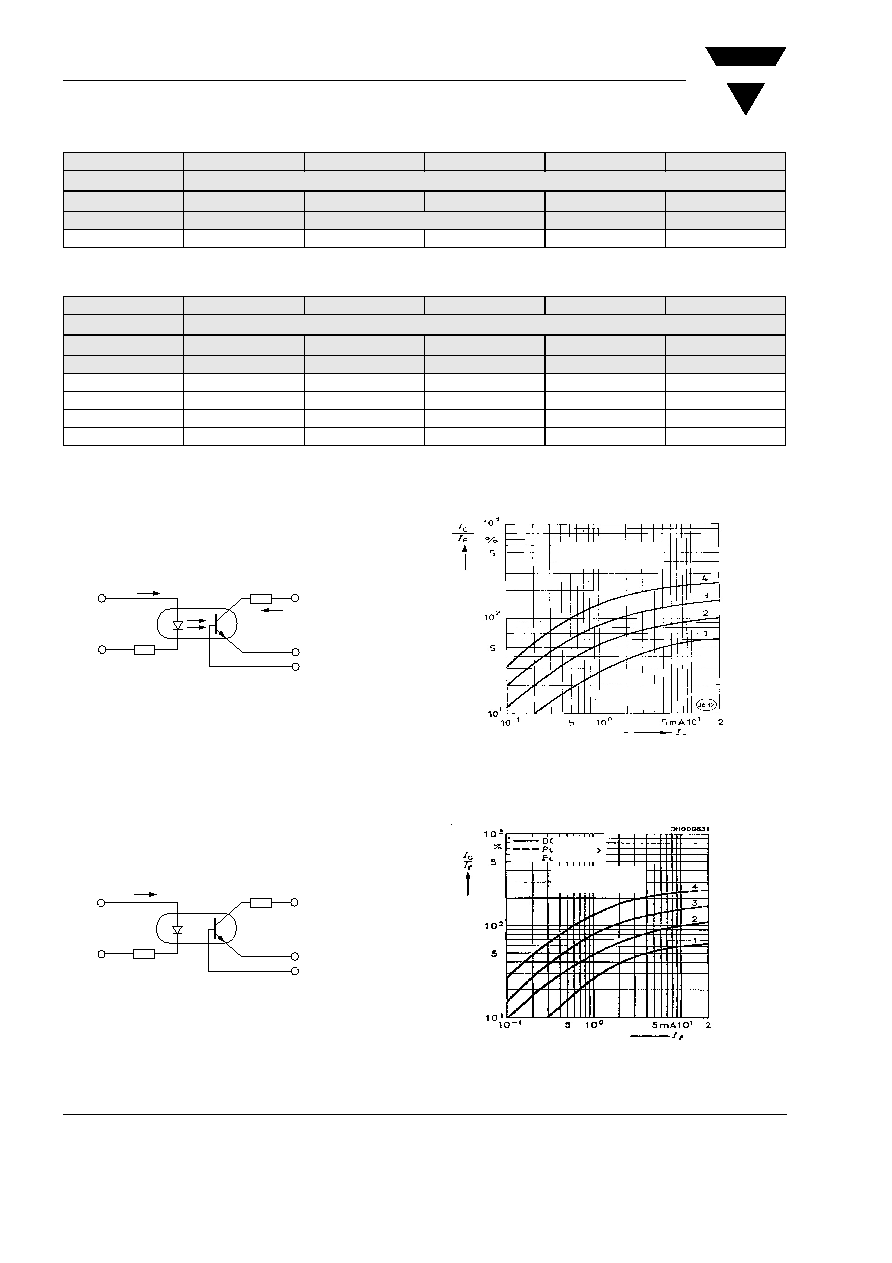
Figure 3. Current Transfer Ratio vs. Diode Current
Figure 4. Current Transfer Ratio vs. Diode Current
(TA = ≠25∞C, VCE = 5.0 V)
IC/IF = f (IF)
isfh600_03
DC
Pulsbetrieb
Pulse
(TA = 0∞C, VCE = 5.0 V)
IC/IF = f (IF)
isfh601_04
VISHAY
SFH601
Document Number 83663
Rev. 1.4, 26-Oct-04
Vishay Semiconductors
www.vishay.com
5
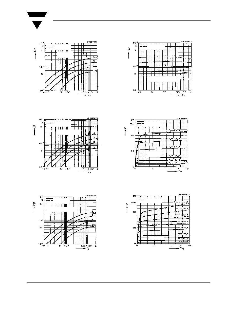
Figure 5. Current Transfer Ratio vs. Diode Current
Figure 6. Current Transfer Ratio vs. Diode Current
Figure 7. Current Transfer Ratio vs. Diode Current
DC
Pulsbetrieb
Pulse
(VCE = 5.0 V)
IC/IF = f (IF)
isfh601_05
DC
Pulsbetrieb
Pulse
(TA = 50∞C, VCE = 5.0 V)
IC/IF = f (IF)
isfh601_06
DC
Pulsbetrieb
Pulse
(TA = 75∞C, VCE = 5.0 V)
IC/IF = f (IF)
isfh601_07
Figure 8. Current Transfer Ratio vs. Diode Current
Figure 9. Transistor Characteristics
Figure 10. Output Characteristics
DC
Pulsbetrieb
Pulse
(IF = 10 mA, VCE = 5.0 V)
IC/IF = f (T)
isfh601_08
DC
Pulsbetrieb
Pulse
IC = f (VCE)
(IF = 0)
isfh601_09
DC
Pulsbetrieb
Pulse
IC=f(VCE)
isfh601_10