 | –≠–ª–µ–∫—Ç—Ä–æ–Ω–Ω—ã–π –∫–æ–º–ø–æ–Ω–µ–Ω—Ç: SFH6139 | –°–∫–∞—á–∞—Ç—å:  PDF PDF  ZIP ZIP |
SFH6138/ SFH6139
Document Number 83669
Rev. 1.5, 26-Oct-04
Vishay Semiconductors
www.vishay.com
1
i179082
1
2
3
4
8
7
6
5
VCC
VB
V0
GND
NC
A
C
NC
Pb
Pb-free
e3
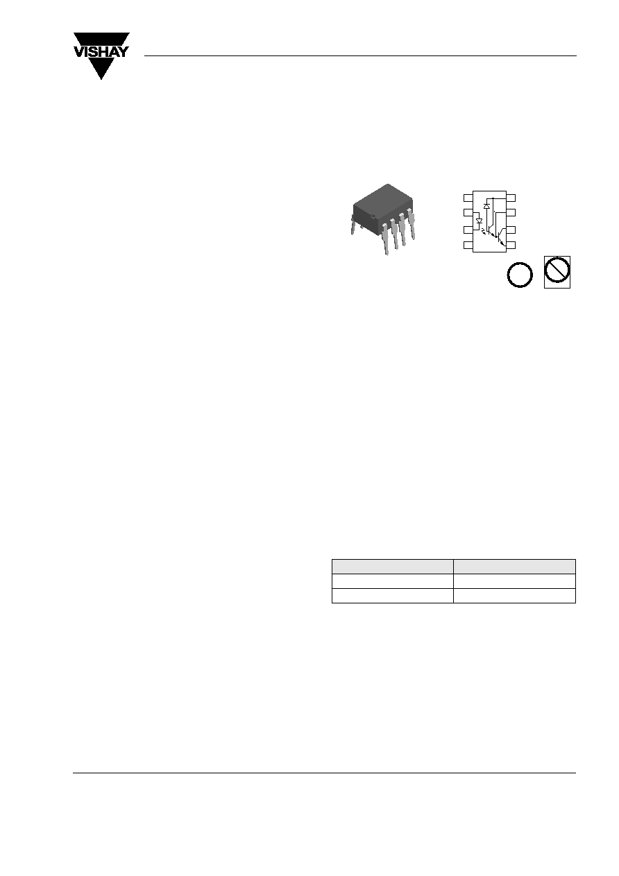
High Speed Optocoupler, 100 kBd, Low Input Current, High Gain
Features
∑ High Current Transfer Ratio, 800 %
∑ Low Input Current Requirement, 0.5 mA
∑ High Output Current, 60 mA
∑ Isolation Test Voltage, 5300 V
RMS
∑ TTL Compatible Output, 0.1 V V
OL
∑ High Common Mode Rejection, 500 V/
µs
∑ DC to 0.1 Megabit/Sec. Operation
∑ Adjustable Bandwidth-Access to Base
∑ Standard Molded Dip Plastic Package
∑ Lead-free component
∑ Component in accordance to RoHS 2002/95/EC
and WEEE 2002/96/EC
Agency Approvals
∑ UL1577, File No. E52744 System Code H or J,
Double Protection
∑ DIN EN 60747-5-2 (VDE0884)
DIN EN 60747-5-5 pending
Available with Option 1
Applications
Logic Ground Isolation-TTL/TTL, TTL/CMOS, CMOS/
CMOS, CMOS/TTL
EIA RS 232C Line Receiver
Low Input Current Line Receiver-Long Lines, Party
Lines
Telephone Ring Detector
117 VAC Line Voltage Status Indication-Low Input
Power Dissipation
Low Power Systems-Ground Isolation
Description
High common mode transient immunity and very high
current ratio together with 5300 V
RMS
insulation are
achieved by coupling an LED with an integrated high
gain photon detector in an eight pin dual-in-line pack-
age. Separate pins for the photo diode and output
stage enable TTL compatible saturation voltages with
high speed operation.
Photodarlington operation is achieved by tying the
V
CC
and V
O
terminals together. Access to the base
terminal allows adjustment to the gain bandwidth.
The SFH6138 is ideal for TTL applications since the
300 % minimum current transfer ratio with an LED
current of 1.6 mA enables operation with one unit
load-in and one unit load-out with a 2.2 k
pull-up
resistor.
The SFH6139 is best suited for low power logic appli-
cations involving CMOS and low power TTL. A 400 %
current transfer ratio with only 0.5 mA of LED current
is guaranteed from 0 ∞C to 70 ∞C.
Order Information
For additional information on the available options refer to
Option Information.
Part
Remarks
SFH6138
CTR
300 %, DIP-8
SFH6139
CTR
400 %, DIP-8
www.vishay.com
2
Document Number 83669
Rev. 1.5, 26-Oct-04
SFH6138/ SFH6139
Vishay Semiconductors
Absolute Maximum Ratings
T
amb
= 25 ∞C, unless otherwise specified
Stresses in excess of the absolute Maximum Ratings can cause permanent damage to the device. Functional operation of the device is
not implied at these or any other conditions in excess of those given in the operational sections of this document. Exposure to absolute
Maximum Rating for extended periods of the time can adversely affect reliability.
Input
Output
Coupler
Parameter
Test condition
Symbol
Value
Unit
Reverse input voltage
5.0
V
Average input current
I
F(AVG)
20
mA
Peak input current
50 % Duty cycle - 1.0 ms pulse
width
40
mA
Peak transient input current
1.0 µs, 300 pps
1.0
A
Parameter
Test condition
Part
Symbol
Value
Unit
Supply and output voltage
V
CC
(pin 8-5), V
O
(pin 6-5)
SFH6138
V
S
, V
O
- 0.5 to 7.0
V
SFH6139
V
S
, V
O
- 0.5 to 18
V
Emitter-base reverse voltage
(pin 5-7)
V
EBO
0.5
V
Output current IO (pin 6)
I
O
60
mA
Derate linearly above 25 ∞C,
free air temperature
0.7
mA/∞C
Input power dissipation
P
diss IN
35
mW
Derate linearly
above 50 ∞C, free air
temperature at 0.7 mW/∞C
Output power dissipation
P
diss OUT
100
mW
Derate linearly
above 25 ∞C, free air
temperature at 0.2 mA/∞C
Parameter
Test condition
Symbol
Value
Unit
Isolation test voltage
t = 1.0 s
V
ISO
5300
V
RMS
Isolation resistance
V
IO
= 500 V, T
amb
= 100 ∞C
R
IO
10
11
V
IO
= 500 V, T
amb
= 25 ∞C
R
IO
10
12
Lead soldering temperature
t = 10 s
T
sld
260
∞C
Storage temperature
T
stg
- 55 to + 125
∞C
SFH6138/ SFH6139
Document Number 83669
Rev. 1.5, 26-Oct-04
Vishay Semiconductors
www.vishay.com
3
Electrical Characteristics
T
amb
= 25 ∞C, unless otherwise specified
Minimum and maximum values are testing requirements. Typical values are characteristics of the device and are the result of engineering
evaluation. Typical values are for information only and are not part of the testing requirements.
Input
Output
2)
Pin 7 open.
Coupler
3)
Device considered a two-terminal device: pins 1, 2, 3 and 4 shorted together and pins 5, 6, 7, and 8 shorted together.
Current Transfer Ratio
1)
DC current transfer ratio is defined as the ratio of output collector current, I
O
, to the forward LED input current, I
F
times 100 %
2)
Pin 7 open.
Parameter
Test condition
Symbol
Min
Typ.
Max
Unit
Input forward voltage
I
F
= 1.6 mA
V
F
1.4
1.7
V
Input reverse breakdown
voltage
I
R
= 10
µA
BV
R
5.0
V
Temperature coefficient of
forward voltage
I
F
= 1.6 mA
- 1.8
mV/∞C
Parameter
Test condition
Part
Symbol
Min
Typ.
Max
Unit
Logic low-output voltage
2)
I
F
= 1.6 mA, I
O
= 4.8 mA,
V
CC
= 4.5 V
SFH6138
V
OL
0.1
0.4
V
I
F
= 1.6 mA, I
O
= 8.0 mA,
V
CC
= 4.5 V
SFH6139
V
OL
0.1
0.4
V
Logic low-output voltage
I
F
= 5.0 mA, I
O
= 15 mA,
V
CC
= 4.5 V
SFH6139
V
OL
0.15
0.4
V
I
F
= 12 mA, I
O
= 24 mA,
V
CC
= 4.5 V
SFH6139
V
OL
0.25
0.4
V
Logic high-output current
2)
I
F
= 0 mA, V
O
= V
CC
= 7.0 V
SFH6138
I
OH
0.1
250
µA
I
F
= 0 mA, V
O
= V
CC
= 18 V
SFH6139
I
OH
0.05
100
µA
Logic low supply current
2)
I
F
= 1.6 mA, V
O
= OPEN,
V
CC
= 18 V
I
CCL
0.2
1.5
mA
Logic high supply current
I
F
= 0 mA, V
O
= OPEN,
V
CC
= 18 V
I
CCH
0.001
10
µA
Parameter
Test condition
Symbol
Min
Typ.
Max
Unit
Input capacitance
f = 1.0 MHz, V
F
= 0
C
IN
25
pF
Capacitance (input-output)
3)
f = 1.0 MHz
C
O
0.6
pF
Parameter
Test condition
Part
Symbol
Min
Typ.
Max
Unit
Current Transfer Ratio
1,2)
I
F
= 1.6 mA, V
O
= 0.4 V,
V
CC
= 4.5 V
SFH6138
CTR
300
1600
%
I
F
= 0.5 mA, V
O
= 0.4 V,
V
CC
= 4.5 V
SFH6139
CTR
400
1600
%
Current Transfer Ratio
I
F
= 1.6 mA, V
O
= 0.4 V,
V
CC
= 4.5 V
SFH6139
CTR
500
2000
%
www.vishay.com
4
Document Number 83669
Rev. 1.5, 26-Oct-04
SFH6138/ SFH6139
Vishay Semiconductors
Switching Characteristics
Delay Time
2)
Pin 7 open.
4)
Using a resistor between pin 5 and 7 will decrease gain and delay time.
Common Mode Transient Immunity
5)
Common mode transient immunity in logic high level is the maximum tolerable (positive) dV
cm
/dt on the leading edge of the common
mode pulse, V
CM
, to assure that the output will remain in a logic high state (i.e.V
O
> 2.0 V) common mode transient immunity in logic low
level is the maximum tolerable (negative) dV
cm
/dt on the trailing edge of the common mode pulse signal, V
CM
, to assure that the output
will remain in a logic low state (i.e. V
O
< 0.8 V).
6)
In applications where dv/dt may exceed 50,000 V/
µs (such as state discharge a series resistor, R
CC
should be included to protect I
C
from destructively high surge currents. The recommended value is R
CC
[IV / 0.15 I
F
(mA)] K
Parameter
Test condition
Part
Symbol
Min
Typ.
Max
Unit
Propagation delay time to logic
low at output
I
F
= 1.6 mA, R
L
= 2.2 k
SFH6138
t
PHL
2.0
10
µs
I
F
= 0.5 mA, R
L
= 4.7 k
SFH6139
t
PHL
6.0
25
µs
I
F
= 12 mA, R
L
= 270 k
SFH6139
t
PHL
0.6
1.0
µs
Propagation delay time to logic
high at output
2.4)
I
F
= 1.6 mA, R
L
= 2.2 k
SFH6138
t
PLH
4.0
35
µs
I
F
= 0.5 mA, R
L
= 4.7 k
SFH6139
t
PLH
5.0
60
µs
I
F
= 12 mA, R
L
= 270 k
SFH6139
t
PLH
1.0
7.0
µs
Parameter
Test condition
Symbol
Min
Typ.
Max
Unit
Common mode transient
immunity at logic high level
output
5,6)
I
F
= 0 mA, R
L
= 2.2 k
,
R
CC
= 0/V
CM
= 10 V
P-P
CM
H
500
V/
µs
Common mode transient
immunity at logic low level
output
5,6)
I
F
= 16 mA, R
L
= 2.2 k
,
R
CC
= 0/V
CM
= 10 V
P-P
CM
L
- 500
V/
µs
SFH6138/ SFH6139
Document Number 83669
Rev. 1.5, 26-Oct-04
Vishay Semiconductors
www.vishay.com
5
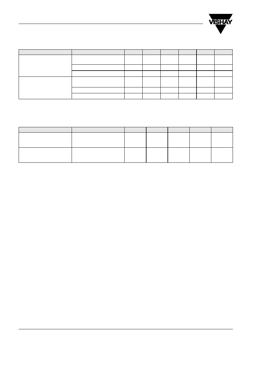
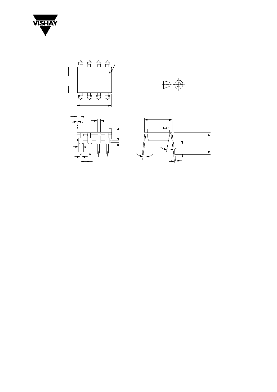
Package Dimensions in Inches (mm)
i178006
pin one ID
.255 (6.48)
.268 (6.81)
.379 (9.63)
.390 (9.91)
.030 (0.76)
.045 (1.14)
4∞ typ.
.100 (2.54) typ.
10∞
3∞≠9∞
.300 (7.62)
typ.
.018 (.46)
.022 (.56)
.008 (.20)
.012 (.30)
.110 (2.79)
.130 (3.30)
.130 (3.30)
.150 (3.81)
.020 (.51 )
.035 (.89 )
.230(5.84)
.250(6.35)
4
3
2
1
.031 (0.79)
.050 (1.27)
5
6
7
8
ISO Method A