Document Number: 83673
www.vishay.com
Revision 17-August-01
2≠242
FEATURES
∑ Very High CTR at
I
F
=1.0 mA,
V
CE
=0.5 V
≠ SFH618A-2, 63≠125%
≠ SFH618A-3, 100≠200%
≠ SFH618A-4, 160≠320%
≠ SFH618A-5, 250≠500%
≠ SFH628A-2, 63≠200%
≠ SFH628A-3, 100≠320%
≠ SFH628A-4, 160≠500%
∑ Specified Minimum CTR at
I
F
=0.5 mA
≠ SFH618A,
V
CE
=1.5 V:
32% (typical 120%)
≠ SFH628A,
V
CE
=1.5 V:
50% (typical 160%)
∑ Good CTR Linearity Depending on
Forward Current
∑ Low CTR Degradation
∑ High Collector-emitter Voltage,
V
CEO
=55 V
∑ Isolation Test Voltage, 5300 V
RMS
∑ Low Coupling Capacitance
∑ Field-Effect Stable by TRIOS (TRansparent IOn
Shield)
∑ End-Stackable, 0.100" (2.54 mm) Spacing
∑ High Common-mode Interference Immunity
(Unconnected Base)
∑ Underwriters Lab File #52744
∑ VDE 0884 Available with Option 1
∑ SMD Option -- See SFH6186/6286 Data Sheet
APPLICATIONS
∑ Telecom
∑ Industrial Controls
∑ Battery Powered Equipment
∑ Office Machines
DESCRIPTION
The SFH618A/628A feature a high current transfer
ratio, low coupling capacitance and high isolation
voltage. These couplers have a GaAs infrared emit-
ting diode emitter, which is optically coupled to a sili-
con planar phototransistor detector, and is
incorporated in a plastic DIP-4 package.
The coupling devices are designed for signal trans-
mission between two electrically separated circuits.
The couplers are end-stackable with 2.54 mm lead
spacing.
Creepage and clearance distances of >8.0 mm are
achieved with option 6. This version complies with
IEC 950 (DIN VDE 0805) for reinforced insulation up
to an operation voltage of 400 V
RMS
or DC.
V
D E
SFH618A/628A
Phototransistor, 5.3 kV TRIOS
Low Current Input
Optocoupler
Maximum Ratings
Emitter
Reverse Voltage (SFH618A) ............................................................. 6.0 V
DC Forward Current (SFH628A) .................................................. ±50 mA
Surge Forward Current (t
p
10 µs) (SFH628A) ............................... ±2.5 A
Total Power Dissipation ................................................................. 70 mW
Detector
Collector-emitter Voltage ................................................................... 55 V
Emitter-collector Voltage................................................................... 7.0 V
Collector Current ............................................................................ 50 mA
Collector Current (t
p
1.0 ms) ....................................................... 100 mA
Total Power Dissipation ............................................................... 150 mW
Package
Isolation Test Voltage between Emitter and
Detector, refer to Climate DIN 40046,
part 2, Nov. 74 ..................................................................... 5300 V
RMS
Creepage Distance ....................................................................
7.0 mm
Clearance ...................................................................................
7.0 mm
Insulation Thickness between Emitter and Detector ..................
0.4 mm
Comparative Tracking Index
per DIN IEC 112/VDE0 303, part 1 ..................................................175
Isolation Resistance
V
IO
=500 V,
T
A
=25
∞
C.................................................................
10
12
V
IO
=500 V,
T
A
=100
∞
C...............................................................
10
11
Storage Temperature Range ............................................. ≠55 to +150
∞
C
Ambient Temperature Range............................................. ≠55 to +100
∞
C
Junction Temperature ......................................................................100
∞
C
Soldering Temperature (max. 10 s. Dip Soldering
Distance to Seating Plane
1.5 mm) ..........................................260
∞
C
Dimensions in Inches (mm)
.255 (6.48)
.268 (6.81)
1
2
4
3
.179 (4.55)
.190 (4.83)
pin one ID
.030 (.76)
.045 (1.14)
4
∞
typ.
0.100 (2.54)
.130 (3.30)
.150 (3.81)
.020 (.508 )
.035 (.89)
10
∞
3
∞≠9∞
.018 (.46)
.022 (.56)
.008 (.20)
.012 (.30)
.031 (.79) typ.
.050 (1.27) typ.
.300 (7.62) typ.
.110 (2.79)
.130 (3.30)
.230 (5.84)
.250 (6.35)
.050 (1.27)
Collector
Emitter
Anode
Cathode
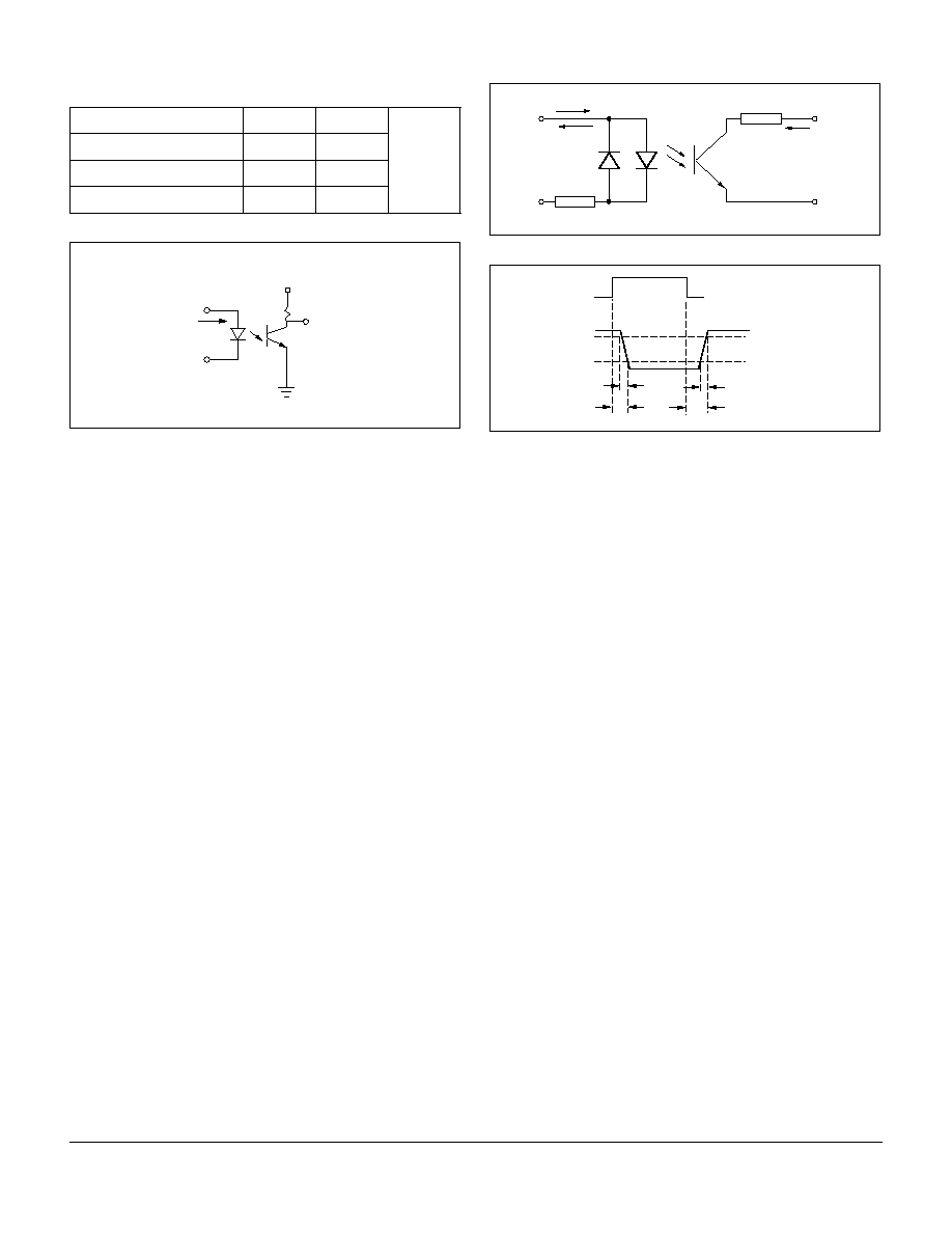
SFH618A
1
2
4
3
Collector
Emitter
Anode/
Cathode
Cathode/
Anode
SFH628A
1
2
4
3
Document Number: 83673
www.vishay.com
Revision 17-August-01
2≠244
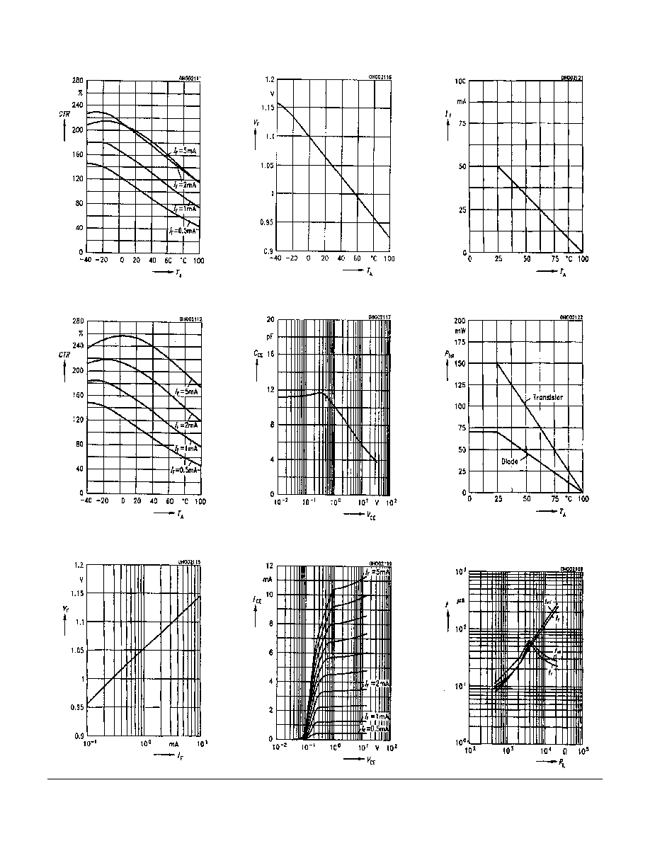
Figure 1. Current Transfer Ratio (typ.)
V
CE
=0.5 V, C
TR
=f(T
A
)
Figure 2. Current Transfer Ratio (typ.)
V
CE
=1.5 V, C
TR
=f(T
A
)
Figure 3. Diode Forward Voltage
T
A
=25
∞C, V
F
=f(I
F
)
Figure 4. Diode Forward Voltage
I
F
=1.0 mA, V
F
=f(T
A
)
Figure 5. Transistor Capacitance
T
A
=25
∞C, f=1.0 MHz, C
CE
=f(V
CE
)
Figure 6. Output Characteristics
T
A
=25
∞C, C
E
=f(V
CE
, I
F
)
Figure 7. Permissible Forward Current
Diode I
F
=f(T
A
)
Figure 8. Permissible Power
Dissipation P
tot
=f(T
A
)
Figure 9. Switching Times (typ.)
T
A
=25
∞C, I
F
=1.0 mA, V
CC
=5.0 V
t
on
, t
r,
t
off
, t
f
=f(R
L
)