 | –≠–ª–µ–∫—Ç—Ä–æ–Ω–Ω—ã–π –∫–æ–º–ø–æ–Ω–µ–Ω—Ç: SFH690ABT | –°–∫–∞—á–∞—Ç—å:  PDF PDF  ZIP ZIP |
SFH690ABT/ AT/ BT/ CT
Document Number 83686
Rev. 1.5, 20-Apr-04
Vishay Semiconductors
www.vishay.com
1
i179065
1
2
4
3
E
C
A
C
Pb
Pb-free
e3
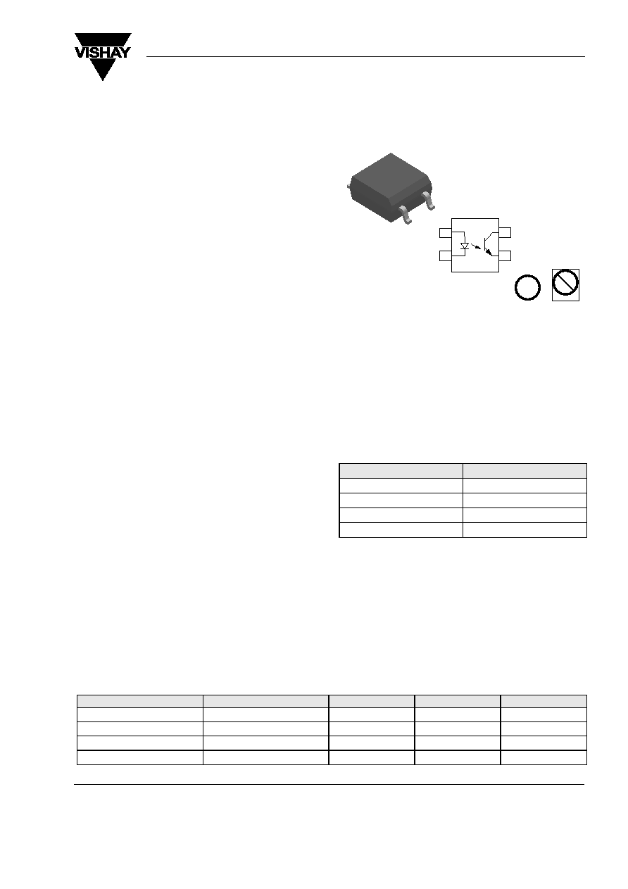
Optocoupler, Phototransistor Output, SOP-4, Mini-Flat Package
Features
∑ SOP (Small Outline Package)
∑ Isolation Test Voltage, 3750 V
RMS
(1.0 s)
∑ High Collector-Emitter Breakdown Voltage,
V
CEO
= 70 V
∑ Low Saturation Voltage
∑ Fast Switching Times
∑ Temperature Stable
∑ Low Coupling Capacitance
∑ End-Stackable, .100 " (2.54 mm) Spacing
∑ Lead-free component
∑ Component in accordance to RoHS 2002/95/EC
and WEEE 2002/96/EC
Agency Approvals
∑ UL1577, File No. E52744 System Code U
∑ CSA 93751
∑ BSI IEC60950 IEC60065
Applications
High density mounting or space sensitive PCBs
PLCs
Telecommunication
Description
The SFH690ABT/ AT/ BT/ CT family has a GaAs
infrared emitting diode emitter, which is optically cou-
pled to a silicon planar phototransistor detector, and
is incorporated in a 4-pin 100 mil lead pitch miniflat
package. It features a high current transfer ratio, low
coupling capacitance, and high isolation voltage.
The coupling devices are designed for signal trans-
mission between two electrically separated circuits.
The SFH690 series is available only on tape and reel.
There are 2000 parts per reel. Marking for SFH690AT
is SFH690A; SFH690BT is SFH690B; SFH690CT is
SFH690C; SFH690ABT will be marked as SFH690A
or SFH690B.
Order Information
For additional information on the available options refer to
Option Information.
Absolute Maximum Ratings
T
amb
= 25 ∞C, unless otherwise specified
Stresses in excess of the absolute Maximum Ratings can cause permanent damage to the device. Functional operation of the device is
not implied at these or any other conditions in excess of those given in the operational sections of this document. Exposure to absolute
Maximum Rating for extended periods of the time can adversely affect reliability.
Input
Part
Remarks
SFH690ABT
CTR 50 - 300 %, SMD-4
SFH690AT
CTR 50 - 150 %, SMD-4
SFH690BT
CTR 100 - 300 %, SMD-4
SFH690CT
CTR 100 - 200 %, SMD-4
Parameter
Test condition
Symbol
Value
Unit
Reverse voltage
V
R
6.0
V
DC Forward current
I
F
50
mA
Surge forward current
t
p
10 µs
I
FSM
2.5
A
Power dissipation
P
diss
80
mW
www.vishay.com
2
Document Number 83686
Rev. 1.5, 20-Apr-04
SFH690ABT/ AT/ BT/ CT
Vishay Semiconductors
Output
Coupler
Parameter
Test condition
Symbol
Value
Unit
Collector-emitter voltage
V
CE
70
V
Emitter-collector voltage
V
EC
7.0
V
Collector current
I
C
50
mA
t
p
1.0 ms
I
C
100
mA
Power dissipation
P
diss
150
mW
Parameter
Test condition
Symbol
Value
Unit
Isolation test voltage between
emitter and detector (1.0 s)
V
ISO
3750
V
RMS
Creepage
5.33
mm
Clearance
5.08
mm
Insulation thickness between
emitter and detector
0.4
mm
Comparative tracking index per
DIN IEC 112/VDEO 0303, part 1
175
Isolation resistance
V
IO
= 500 V, T
amb
= 25 ∞C
R
IO
10
12
V
IO
= 500 V, T
amb
= 100 ∞C
R
IO
10
11
Storage temperature range
T
stg
- 55 to + 150
∞C
Ambient temperature range
T
amb
- 55 to + 100
∞C
Junction temperature
T
j
100
∞C
Soldering temperature
max. 10 s Dip soldering distance
to seating plane
1.5 mm
T
sld
260
∞C
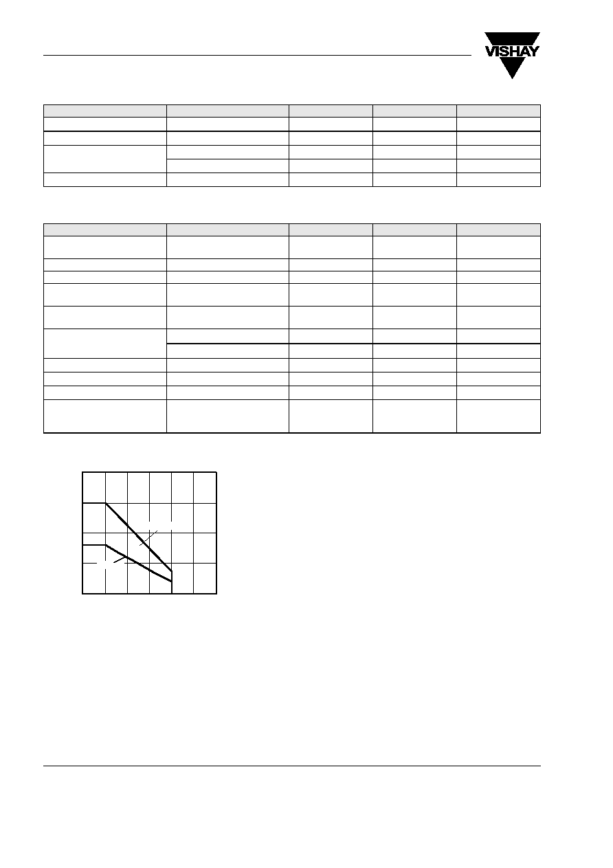
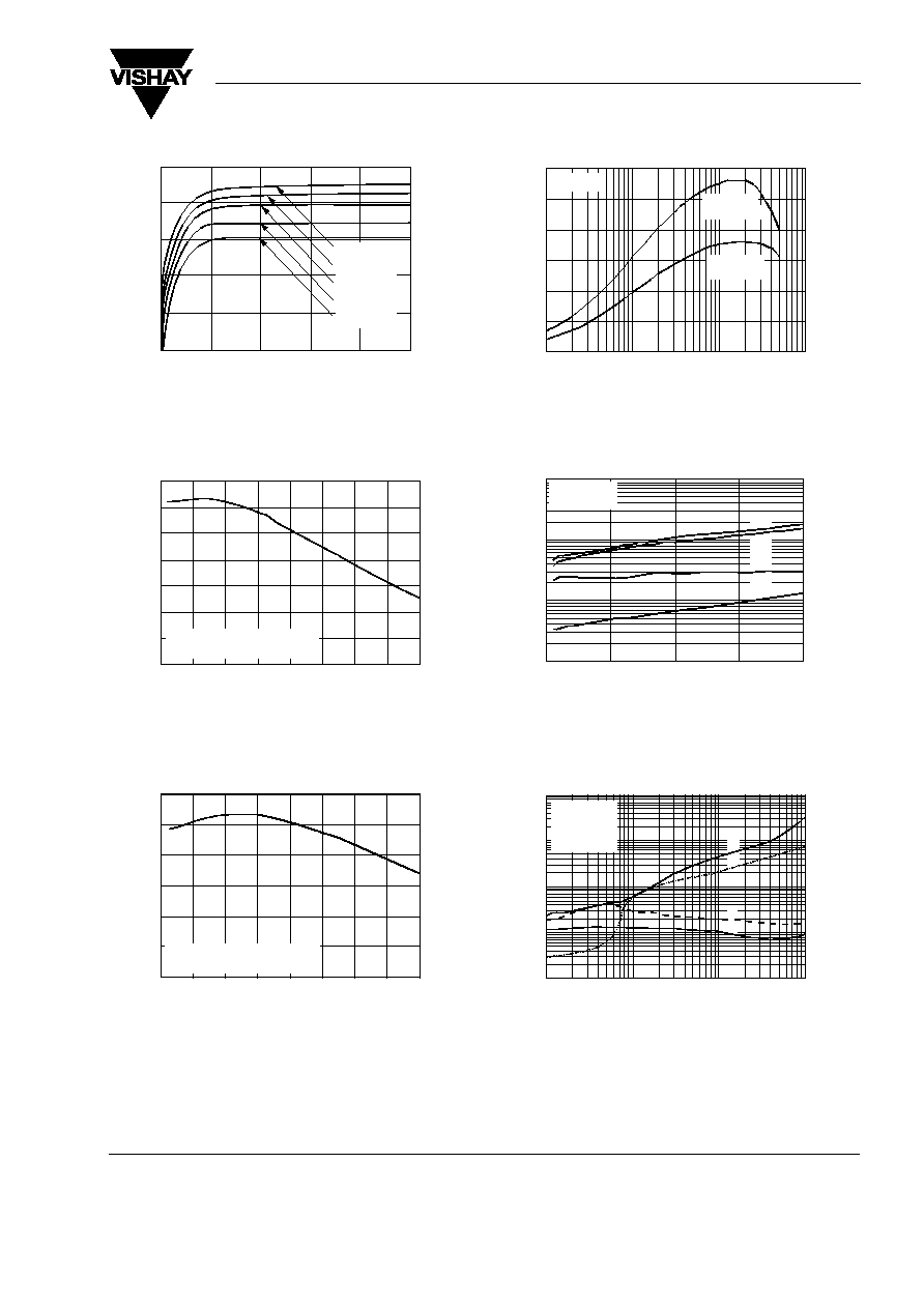
Figure 1. Permissible Power Dissipation vs. Ambient Temperature
0
50
100
150
200
0
25
50
75
100
125
150
18484
P
≠Power Dissipation (mW)
tot
Phototransistor
Diode
T
amb
≠ Ambient Temperature ( C )
SFH690ABT/ AT/ BT/ CT
Document Number 83686
Rev. 1.5, 20-Apr-04
Vishay Semiconductors
www.vishay.com
3
Electrical Characteristics
T
amb
= 25 ∞C, unless otherwise specified
Minimum and maximum values are testing requirements. Typical values are characteristics of the device and are the result of engineering
evaluation. Typical values are for information only and are not part of the testing requirements.
Input
Output
Coupler
Current Transfer Ratio
Parameter
Test condition
Symbol
Min
Typ.
Max
Unit
Forward voltage
I
F
= 5 mA
V
F
1.15
1.4
V
Reverse current
V
R
= 6.0 V
I
R
0.01
10
µA
Capacitance
V
R
= 0.0 V, f = 1.0 MHz
C
O
14
pF
Thermal resistance
R
thja
750
K/W
Parameter
Test condition
Symbol
Min
Typ.
Max
Unit
Collector-emitter leakage
current
V
CE
= 20 V
I
CEO
100
nA
Collector-emitter capacitance
V
CE
= 5.0 V, f = 1.0 MHz
C
CE
2.8
pF
Thermal resistance
R
thja
500
K/W
Parameter
Test condition
Symbol
Min
Typ.
Max
Unit
Collector-emitter saturation
voltage
I
F
= 10 mA, I
C
= 2.0 mA
V
CEsat
0.1
0.3
V
Coupling capacitance
f = 1.0 MHz
C
C
0.3
pF
Parameter
Test condition
Part
Symbol
Min
Typ.
Max
Unit
I
C
/I
F
I
F
= 5.0 mA, V
CE
= 5.0 V SFH690AT
CTR
50
150
%
SFH690BT
CTR
100
300
%
SFH690CT
CTR
100
200
%
SFH690ABT
CTR
50
300
%
www.vishay.com
4
Document Number 83686
Rev. 1.5, 20-Apr-04
SFH690ABT/ AT/ BT/ CT
Vishay Semiconductors
Switching Characteristics
Typical Characteristics (Tamb = 25
∞C unless otherwise specified)
Parameter
Test condition
Symbol
Min
Typ.
Max
Unit
Rise time
I
C
= 2.0 mA, V
CC
= 5.0 V,
R
L
= 100
t
r
3.0
µs
Fall time
I
C
= 2.0 mA, V
CC
= 5.0 V,
R
L
= 100
t
f
4.0
µs
Turn-on time
I
C
= 2.0 mA, V
CC
= 5.0 V,
R
L
= 100
t
on
5.0
µs
Turn-off time
I
C
= 2.0 mA, V
CC
= 5.0 V,
R
L
= 100
t
off
3.0
µs
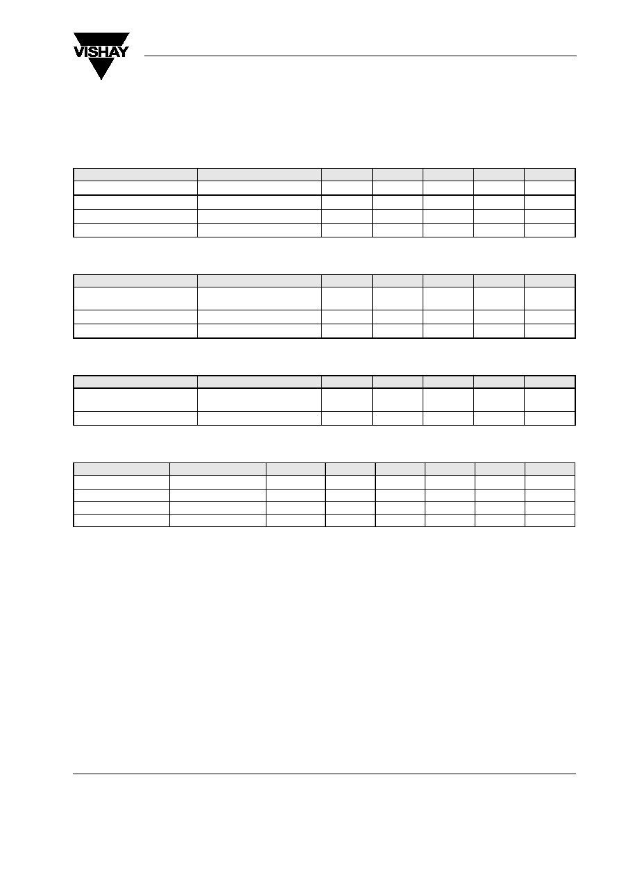
Figure 2. Switching Operation (without Saturation)
Figure 3. Diode Forward Voltage vs. Forward Current
isfh690at_01
RL = 100
V
CC
= 5 V
50
I
F
isfh690at_02
Forward
Voltage,
V
F
(V)
Forward Current, IF (mA)
0.01
0.10
1.00
10.00
100.00
1.6
1.4
1.1
0.9
0.6
T=≠55∞C
T=100∞C
T=75∞C
T=50∞C
T=25∞C
T=≠25∞C
T=0∞C
Figure 4. Collector Current vs. Collector Emitter Voltage
Figure 5. Collector to Emitter Dark Current vs. Ambient
Temperature
isfh690at_03
80
70
60
50
40
30
20
10
0
0
2
4
6
8
10
Collector to Emitter Voltage, VCE (V)
IF = 30 mA
Collector
Current,
I C
(mA)
IF = 20 mA
IF = 15 mA
IF = 5 mA
IF = 10 mA
isfh690at_04
1000.0
100.0
10.0
1.0
≠60
≠40
≠20
0
20
40
60
80 100
12 V
24 V
40 V
Collector-Emitter
Dark
Current,
I CEO
(nA)
Ambient Temperature, TA (∞C)
SFH690ABT/ AT/ BT/ CT
Document Number 83686
Rev. 1.5, 20-Apr-04
Vishay Semiconductors
www.vishay.com
5
Figure 6. Collector Current vs. Collector-Emitter Saturation
Voltage
Figure 7. Normalized Output Current vs. Ambient Temperature
Figure 8. Normalized Output Current vs. Ambient Temperature
isfh690at_05
Collector
Current
(mA)
Collector-Emitter Saturation Voltage, VCE (sat) (V)
100.000
10.000
1.000
0.100
0.010
0.001
0.0
0.2
0.4
0.6
0.8
1.0
IF = 25 mA
IF = 10 mA
IF = 5.0 mA
IF = 2.0 mA
IF = 1.0 mA
isfh690at_06
Normalized
Output
Current,
CTR
1.4
1.2
1.0
0.8
0.6
0.4
0.2
0.0
Ambient Temperature, TA (∞C)
≠60
≠40
≠20
0
20
40
60
80
100
Normalized to 1.0 at TA = 25 ∞C
IF = 1.0 mA, VCE = 5.0 V
isfh690at_07
1.2
1.0
0.8
0.6
0.4
0.2
0.0
Normalized
Output
Current,
CTR
Ambient Temperature, TA (∞C)
≠60
≠40
≠20
0
20
40
60
80
100
Normalized to 1.0 at TA = 25 ∞C
IF = 5.0 mA, VCE = 5.0 V
Figure 9. Current Transfer Ratio vs. Forward Current
Figure 10. Switching Time vs. Load Resistance
Figure 11. Switching Time vs. Load Resistance
isfh690at_08
Current
Transfer
Ratio,
CTR
(%)
Forward Current, IF (mA)
300
250
200
150
100
50
0
0.1
1.0
10.0
50 100.0
VCE=5.0 V
Typical for
CTR=250%
Typical for
CTR=150%
isfh690at_09
Switching
Time
(
µ
s)
Load Resistance, RL ()
100.0
10.0
1.0
0.1
0
500
1000
1500
2000
t on
t off
td
ts
VCC = 5.0 V
IC = 2.0 mA
isfh690at_10
Switching
Time,
(
µ
s)
Load Resistance, RL ()
1000
100
10
1
0
100
1000
10000
100000
IF = 5.0 mA
VCC = 5.0 V
CTR = 150%
t r
td
t s
tf