 | –≠–ª–µ–∫—Ç—Ä–æ–Ω–Ω—ã–π –∫–æ–º–ø–æ–Ω–µ–Ω—Ç: SI91860DY | –°–∫–∞—á–∞—Ç—å:  PDF PDF  ZIP ZIP |
Si9420DY
Siliconix
Vishay-Siliconix, 2201 Laurelwood Road, Santa Clara, CA 95054
S
Phone (408)988-8000
S
FaxBack (408)970-5600
S
www.siliconix.com
S-56996--Rev. G, 03-Aug-98 Siliconix was formerly a division of TEMIC Semiconductors
1
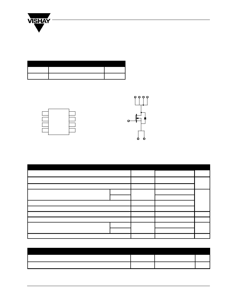
N-Channel Enhancement-Mode MOSFET
PRODUCT SUMMARY
V
DS
(V)
R
DS(ON)
(W)
I
D
(A)
200
1.0 @ V
GS
= 10 V
"
1.0
SO-8
N/C
D
S
D
S
D
G
D
5
6
7
8
Top View
D
2
3
D
4
1
D
G
S
S
D
N-Channel MOSFET
ABSOLUTE MAXIMUM RATINGS (T
A
= 25_C UNLESS OTHERWISE NOTED)
PARAMETER
SYMBOL
LIMIT
UNIT
Drain-Source Voltage
V
DS
200
V
Gate-Source Voltage
V
GS
"
20
V
Continuous Drain Current (T
J
= 150
_
C)
A
T
A
= 25
_
C
I
D
"
1.0
Continuous Drain Current
(T
J
= 150 C)
A
T
A
= 70
_
C
I
D
"
0.8
A
Pulsed Drain Current
I
DM
"
10
A
Avalanche Current
I
AS
5
Single Avalanche Energy
E
AS
1.3
mJ
Continuous Source Current (Diode Conduction)
A
I
S
1.0
A
Maximum Power Dissipation
A
T
A
= 25
_
C
P
D
2.5
W
Maximum Power Dissi ation
A
T
A
= 70
_
C
P
D
1.6
W
Operating Junction and Storage Temperature Range
T
J
, T
stg
≠55 to 150
_
C
THERMAL RESISTANCE RATINGS
PARAMETER
SYMBOL
LIMIT
UNIT
Maximum Junction-to-Ambient
A
R
thJA
50
_
C/W
Notes
A.
Surface Mounted on FR4 Board, t
v
10 sec.
Updates to this data sheet may be obtained via facsimile by calling Siliconix FaxBack, 1-408-970-5600. Please request FaxBack document #70123.
Siliconix
Si9420DY
Vishay-Siliconix, 2201 Laurelwood Road, Santa Clara, CA 95054
S
Phone (408)988-8000
S
FaxBack (408)970-5600
S
www.siliconix.com
S-56996--Rev. G, 03-Aug-98 Siliconix was formerly a division of TEMIC Semiconductors
2
SPECIFICATIONS (T
J
= 25_C UNLESS OTHERWISE NOTED)
PARAMETER
SYMBOL
TEST CONDITION
MIN
TYP
A
MAX
UNIT
STATIC
Gate Threshold Voltage
V
GS(th)
V
DS
= V
GS
, I
D
= 250
m
A
2
V
Gate-Body Leakage
I
GSS
V
DS
= 0 V, V
GS
=
"
20 V
2
"
100
nA
Zero Gate Voltage Drain Current
I
DSS
V
DS
= 160 V, V
GS
= 0 V
2
m
A
Zero Gate Voltage Drain Current
I
DSS
V
DS
= 160 V, V
GS
= 0 V, T
J
= 55
_
C
25
m
A
On-State Drain Current
B
I
D(on)
V
DS
w
10 V, V
GS
= 10 V
5.0
A
Drain-Source On-State Resistance
B
r
DS(on)
V
GS
= 10 V, I
D
= 1.0 A
0.8
1.0
W
Forward Transconductance
B
g
fs
V
DS
= 15 V, I
D
= 1.0 A
1.5
S
Diode Forward Voltage
B
V
SD
I
S
= 1.0 A, V
GS
= 0 V
0.7
1.2
V
DYNAMIC
A
Total Gate Charge
Q
g
8.6
16
Gate-Source Charge
Q
gs
V
DS
= 100 V,
V
GS
= 10 V, I
D
= 1.0 A
1.5
nC
Gate-Drain Charge
Q
gd
3.2
Turn-On Delay Time
t
d(on)
7
14
Rise Time
t
r
V
DD
= 100 V, R
L
= 100
W
12
24
Turn-Off Delay Time
t
d(off)
DD
L
I
D
^
1.0 A, V
GEN
= 10 V, R
G
= 6
W
26
50
ns
Fall Time
t
f
15
30
Source-Drain Reverse Recovery Time
t
rr
I
F
= 1.0 A, di/dt = 100 A/
m
s
130
Notes
A.
Guaranteed by design, not subject to production testing.
B.
Pulse test; pulse width
v
300
m
s, duty cycle
v
2%.
Si9420DY
Siliconix
Vishay-Siliconix, 2201 Laurelwood Road, Santa Clara, CA 95054
S
Phone (408)988-8000
S
FaxBack (408)970-5600
S
www.siliconix.com
S-56996--Rev. G, 03-Aug-98 Siliconix was formerly a division of TEMIC Semiconductors
3
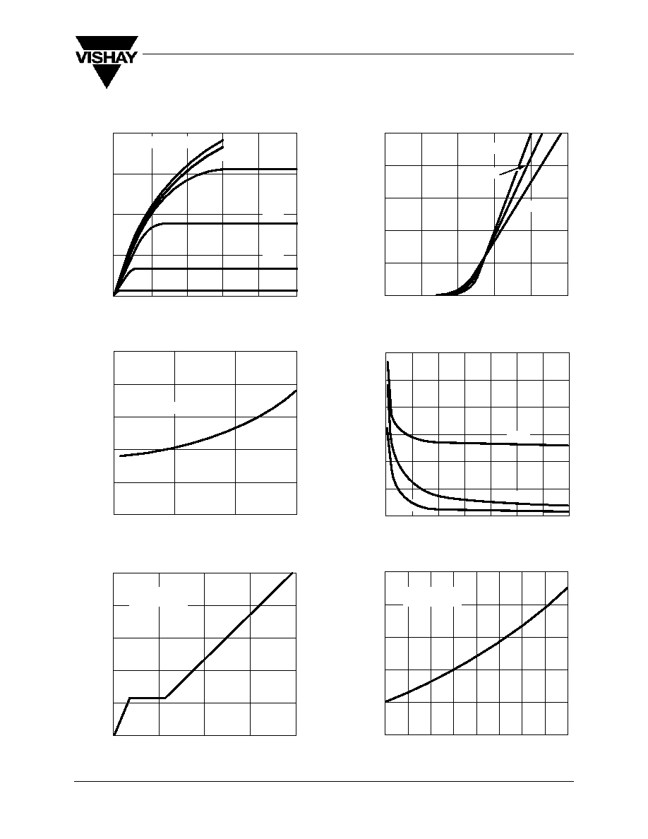
TYPICAL CHARACTERISTICS (25_C UNLESS OTHERWISE NOTED)
Output Characteristics
Transfer Characteristics
Gate Charge
On Resistance vs. Drain Current
V
DS
≠ Drain-to-Source Voltage (V)
≠ Drain Current (A)
I
D
V
GS
≠ Gate-to-Source Voltage (V)
≠ Drain Current (A)
I
D
≠ Gate-to-Source V
oltage
(V)
Q
g
≠ Total Gate Charge (nC)
V
DS
≠ Drain-to-Source Voltage (V)
C ≠ Capacitance (pF)
V
GS
≠ On-Resistance (
r DS(on)
W
)
I
D
≠ Drain Current (A)
Capacitance
On Resistance vs. Junction Temperature
T
J
≠ Junction Temperature (
_
C)
(Normalized)
≠ On-Resistance (
r DS(on)
W
)
0
8
16
20
8
6
4
2
0
4
12
V
GS
= 10, 9 V
8 V
7 V
6 V
5 V
4 V
10
0
2
4
6
8
8
6
4
2
0
10
T
C
= ≠55
_
C
125
_
C
1.40
1.00
0.40
0
2
6
0.80
0.60
4
V
GS
= 10 V
20
16
12
0
0
4
16
8
4
8
12
2.5
2.0
1.5
0
1.0
0.5
≠50
≠25
150
0
25
75
125
100
50
500
400
300
0
0
5
200
100
10
15
25
35
30
20
600
C
rss
C
oss
C
iss
1.20
V
DS
= 100 V
I
D
= 1 A
V
GS
= 10 V
I
D
= 1 A
25
_
C
Siliconix
Si9420DY
Vishay-Siliconix, 2201 Laurelwood Road, Santa Clara, CA 95054
S
Phone (408)988-8000
S
FaxBack (408)970-5600
S
www.siliconix.com
S-56996--Rev. G, 03-Aug-98 Siliconix was formerly a division of TEMIC Semiconductors
4
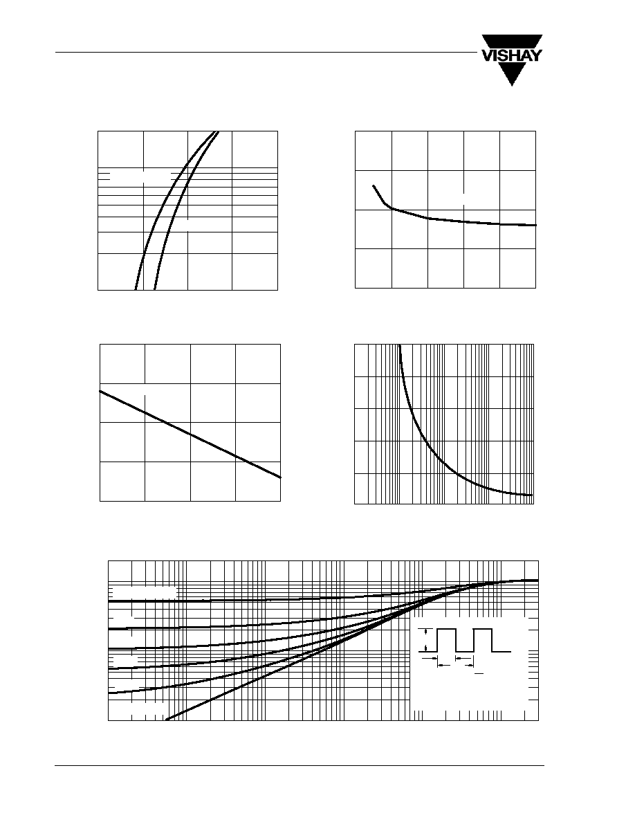
TYPICAL CHARACTERISTICS (25_C UNLESS OTHERWISE NOTED)
Source Drain Diode Forward Voltage
On Resistance vs. Gate to Source Voltage
Threshold Voltage
SinglePulsePower
Normalized Thermal Transient Impedance, Junction to Ambient
Square Wave Pulse Duration (sec)
Normalized Ef
fective
T
ransient
Thermal Impedance
≠ On-Resistance (
r DS(on)
W
)
V
SD
≠ Source-to-Drain Voltage (V)
V
GS
≠ Gate-to-Source Voltage (V)
≠ Source Current (A)
I
S
T
J
≠ Temperature (
_
C)
Time (sec)
Power (W)
0
2
20
10
1
0.5
1.0
1.5
T
J
= 150
_
C
T
J
= 25
_
C
0
0.5
1.0
1.5
2.0
5
6
7
8
9
10
≠1.00
≠0.50
0.00
0.50
1.00
≠50
0
50
100
150
I
D
= 250
m
A
2
1
0.1
0.01
10
≠4
10
≠3
10
≠2
10
≠1
1
10
Duty Cycle = 0.5
0.2
0.1
0.05
0.02
Single Pulse
30
1. Duty Cycle, D =
2. Per Unit Base = R
thJA
= 50
_
C/W
3. T
JM
≠ T
A
= P
DM
Z
thJA
(t)
t
1
t
2
t
1
Notes:
4. Surface Mounted
I
D
= 1 A
P
DM
t
2
0.01
0.1
1
10
100
25
20
15
10
5
0
V
ariance (V)
V
GS(th)