 | –≠–ª–µ–∫—Ç—Ä–æ–Ω–Ω—ã–π –∫–æ–º–ø–æ–Ω–µ–Ω—Ç: SI9243A | –°–∫–∞—á–∞—Ç—å:  PDF PDF  ZIP ZIP |
Si9243AEY
Vishay Siliconix
Document Number: 70788
S-02936--Rev. D, 22-Jan-01
www.vishay.com
1
Single-Ended Bus Transceiver
FEATURES
D
Operating Power Supply Range 6 V
v
V
BAT
v
36 V
D
Reverse Battery Protection Down to V
BAT
w
≠24 V
D
Standby Mode With Very Low Current Consumption
I
BAT(SB)
= 1
m
A @ V
DD
= 0.5 V
D
Low Quiescent Current in OFF Condition
I
BAT
= 120
m
A and I
DD
v
10
m
A
D
ISO 9141 Compatible
D
Overtemperature Shutdown Function For K Output
D
Defined K Output OFF for Open GND
D
Defined Receive Output Status for Open L or K Inputs
D
Defined K Output OFF for TX Input Open
D
2-kV ESD
D
Typical Transmit Speeds of 200 kBaud
DESCRIPTION
The Si9243AEY is a monolithic bus transceiver designed to
provide bidirectional serial communication in automotive
diagnostic applications.
The device incorporates protection against overvoltages and
short circuits to V
BAT
. The transceiver pin is protected and can be
driven beyond the V
BAT
voltage.
The RX output is capable of driving CMOS or 1
LSTTL load.
The Si9243AEY is built on the Vishay Siliconix BiC/DMOS
process. This process supports bipolar transistors, CMOS, and
DMOS. An epitaxial layer prevents latchup.
The Si9243AEY is available in a 8-pin SO package and
operates over the automotive temperature range (≠40 to
125
_
C).
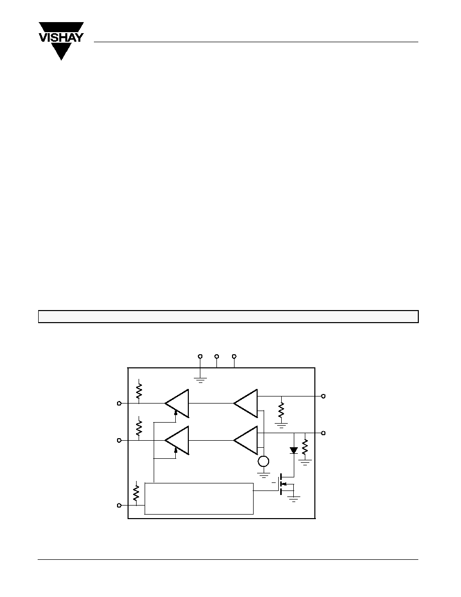
PIN CONFIGURATION AND FUNCTIONAL BLOCK DIAGRAM
TX
RX
L
K
L
+
≠
L
+
≠
K
+
≠
V
BAT
/2
K
Logic and Fault Detect Circuitry
(See State Diagram and Truth Table)
V
BAT
V
DD
GND
RX
K
V
DD
V
DD
V
DD
A = 1
A = 0
Over Temp
Over Temp
@
TX
B = 1
B = 0
Short Circuit
TX
Power On
Power On
Note: Over Temp is an internal condition, not meant
to be a logic signal.
Si9243AEY
Vishay Siliconix
www.vishay.com
2
Document Number: 70788
S-02936--Rev. D, 22-Jan-01
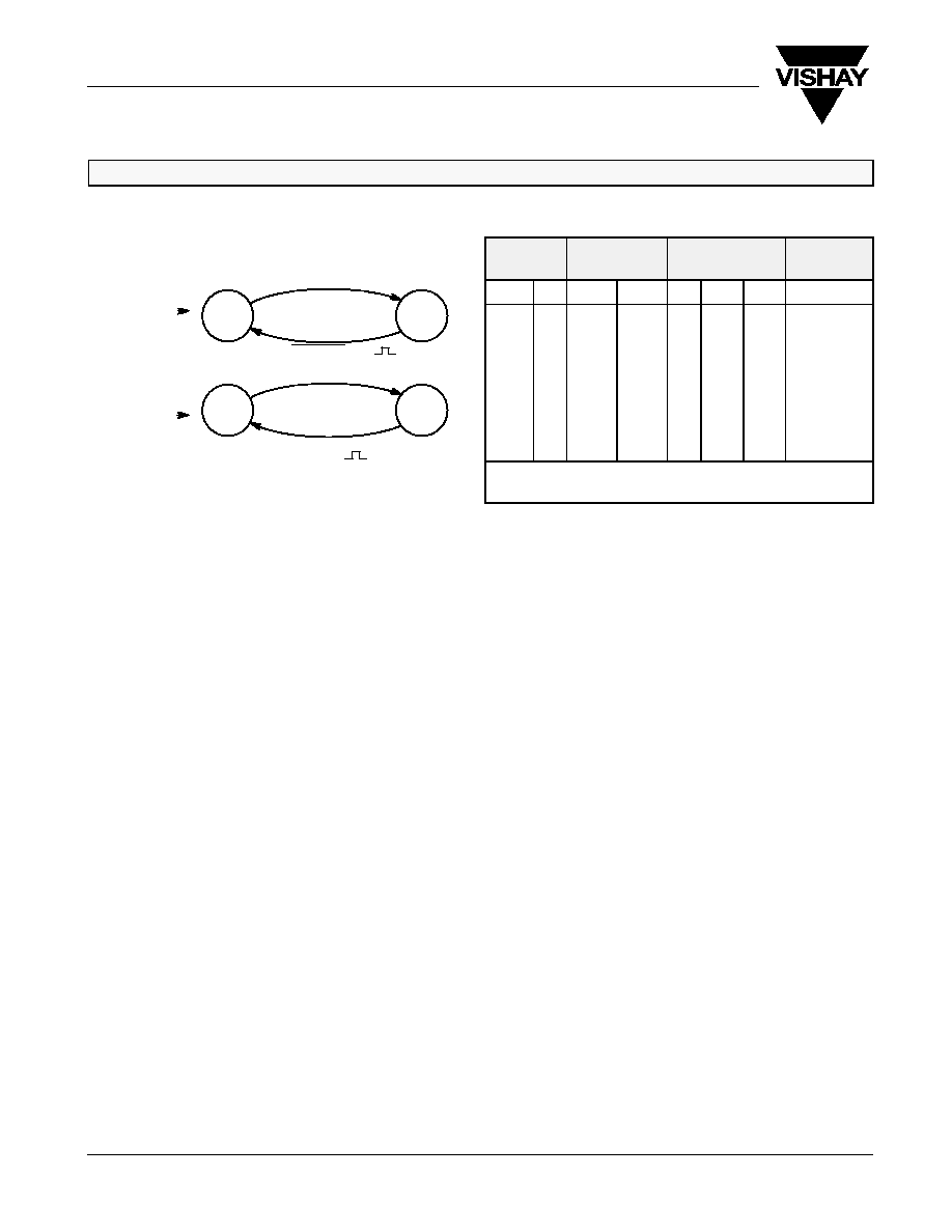
OUTPUT TABLE AND STATE DIAGRAMS
INPUTS
STATE
VARIABLE
OUTPUT
TABLE
TX
L
A
B
K
RX
K
RX
L
Comments
0
0
1
1
0
0
0
1
1
1
1
1
1
1
0
1
1
1
0
0
1
1
0
1
1
1
1
0
X
L
0
1
HiZ
K
L
Over Temp
0
L
1
0
HiZ
K
L
Short Circuit
1
1
1
1
1
1
1
Receive Mode
1
0
1
1
0
0
0
X = "1" or "0"
HiZ = High Impedance State
ABSOLUTE MAXIMUM RATINGS
Voltage Referenced to Ground
Voltage On V
BAT
≠24 V to 45 V
. . . . . . . . . . . . . . . . . . . . . . . . . . . . . . . . . . . . .
Voltage K , L
≠16 V to (V
BAT
+ 1 V)
. . . . . . . . . . . . . . . . . . . . . . . . . . . . . . . . . .
Voltage Difference V
(VBAT, K, L)
55
V
. . . . . . . . . . . . . . . . . . . . . . . . . . . . . . . . .
Voltage On Any Pin (Except V
BAT
, K, L)
or Max. Current
≠0.3 V to (V
DD
+ 0.3 V) or 10 mA
. . . . . . . . . . . . . . . . . . . . . .
Voltage on V
DD
7 V
. . . . . . . . . . . . . . . . . . . . . . . . . . . . . . . . . . . . . . . . . . . . . . . .
K Pin Only, Short Circuit Duration (to V
BAT
or GND)
Continuous
. . . . . . . . . .
Operating Temperature (T
A
)
≠40 to 125
_
C
. . . . . . . . . . . . . . . . . . . . . . . . . . . .
Junction and Storage Temperature
-55 to 150
_
C
. . . . . . . . . . . . . . . . . . . . . .
Thermal Resistance
Q
JA
125
_
C/W
. . . . . . . . . . . . . . . . . . . . . . . . . . . . . . . . . .
Stresses beyond those listed under "Absolute Maximum Ratings" may cause permanent damage to the device. These are stress ratings only, and functional operation
of the device at these or any other conditions beyond those indicated in the operational sections of the specifications is not implied. Exposure to absolute maximum rating
conditions for extended periods may affect device reliability.
RECOMMENDED OPERATING RANGE
Voltage Referenced to Ground
V
DD
4.5 V to 5.5 V
. . . . . . . . . . . . . . . . . . . . . . . . . . . . . . . . . . . . . . . . . . . . . . . . .
V
BAT
6 V to 36 V
. . . . . . . . . . . . . . . . . . . . . . . . . . . . . . . . . . . . . . . . . . . . . . . . . .
K, L
6 V to 36 V
. . . . . . . . . . . . . . . . . . . . . . . . . . . . . . . . . . . . . . . . . . . . . . . . . . .
Digital Inputs
0 to V
DD
. . . . . . . . . . . . . . . . . . . . . . . . . . . . . . . . . . . . . . . . . . . . .
Si9243AEY
Vishay Siliconix
Document Number: 70788
S-02936--Rev. D, 22-Jan-01
www.vishay.com
3
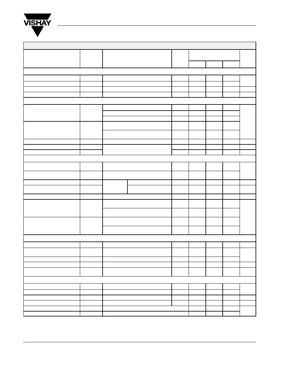
SPECIFICATIONS
Test Conditions Unless Specified
Limits
≠40 to 125
_
C
Parameter
Symbol
V
DD
= 4.5 to 5.5 V
V
BAT
= 6 to 36 V
Temp
a
Min
b
Typ
c
Max
b
Unit
Transmitter and Logic Levels
TX Input Low Voltage
V
ILT
Full
1.5
TX Input High Voltage
V
IHT
Full
3.5
V
TX Input Capacitance
d
C
INT
Full
10
pF
TX Input Pull-up Resistance
R
TX
V
DD
= 5.5 V, TX = 1.5 V, 3.5 V
Full
10
20
40
k
W
K Transmit
R
L
= 510
W
"
5%
, V
BAT
= 6 to 18 V
Full
0.2 V
BAT
K Output Low Voltage
V
OLK
R
L
= 1 k
W
"
5%
, V
BAT
= 16 to 36 V
Full
0.2 V
BAT
OLK
R
L
= 510
W
"
5%
, V
BAT
= 4.5 V
Full
1.2
R
L
= 510
W
"
5%
, V
BAT
= 4.5 to 18 V
Full
0.95
V
BAT
V
K Output High Voltage
V
OHK
R
L
= 1 k
W
"
5%
, V
BAT
= 16 to 36 V
Full
0.95
V
BAT
K Rise, Fall Times
t
r
, t
f
See Test Circuit
Full
9.6
m
s
K Output Sink Resistance
Rsi
Full
110
W
K Output Capacitance
d
C
O
TX = 0 V
Full
20
pF
Receiver
L and K Input High Voltage
V
IH
Full
0.65
V
BAT
L and K Input Hysteresis
c, d
V
HYS
Full
0.05
V
BAT
V
L and K Input Currents
I
IH
V
IH
= V
BAT
Full
20
m
A
RX
L
and RX
K
Output
Low Voltage
V
OLR
TX = 4 V
V
ILK
, V
ILL
= 0.35 V
BAT
I
OLR
= 1 mA
Full
0.4
V
RX
L
and RX
K
Pull-up Resistance
R
RX
Full
5
20
k
W
R
L
= 510
W
"
5%
, V
BAT
= 6 to 18 V
C
L
= 10 nF, See Test Circuit
Full
3
10
RX
K
Turn On Delay
t
d(on)
R
L
= 1 k
W
"
5%
, V
BAT
= 16 to 36 V
C
L
= 4.7 nF, See Test Circuit
Full
3
10
m
R
L
= 510
W
"
5%
, V
BAT
= 6 to 18 V
C
L
= 10 nF, See Test Circuit
Full
3
10
m
s
RX
K
Turn Off Delay
t
d(off)
R
L
= 1 k
W
"
5%
, V
BAT
= 16 to 36 V
C
L
= 4.7 nF, See Test Circuit
Full
3
10
Supplies
Bat Supply Current On
I
BAT(on)
TX = 0 V, V
BAT
v
16 V
Full
1.2
3
mA
Bat Supply Current Off
I
BAT(off)
V
IHT
v
V
TX
, V
IHK
v
V
K
, V
IHL
v
V
L
V
BAT
v
12 V
Full
120
220
m
A
Bat Supply Current Standby
I
BAT(SB)
V
DD
v
0.5 V, V
BAT
v
12 V
Full
t
1
10
m
A
Logic Supply Current On
I
DD(on)
V
DD
v
5.5 V, TX = 0 V
Full
1.4
2.3
mA
Logic Supply Current Off
I
DD(off)
V
IHT
v
V
TX
, V
IHK
v
V
K
, V
IHL
v
V
L
V
BAT
v
12 V
Full
10
mA
Miscellaneous
TX Transmit Baud Rate
BR
T
R
L
= 510
W
, C
L
= 10 nF
Full
10.4
RX
L
and RX
K
Receive Baud Rate
c
BR
R
6 V
t
V
BAT
< 16 V, C
RX
= 20 pF
Full
200
kBaud
Transmission Frequency
f
K-RXK
6 V
t
V
BAT
< 16 V, R
K
= 510
W,
C
K
v
1.3 nF
Full
50
200
kHz
TX Minimum Pulse Width
d, e
t
TX
Full
1
m
s
Over Temperature Shutdown
d
T
SHUT
Temperature Rising
160
180
_
Temperature Shutdown Hysteresis
c
T
HYST
30
_
C
Notes
a.
Room = 25
_
C, Cold and Hot = as determined by the operating temperature suffix.
b.
The algebraic convention whereby the most negative value is a minimum and the most positive a maximum, is used in this data sheet.
c.
Typical values are for DESIGN AID ONLY, not guaranteed nor subject to production testing.
d.
Guaranteed by design, not subject to production test.
e.
Minimum pulse width to reset a fault condition.
1
2
3
4
5
6
7
8
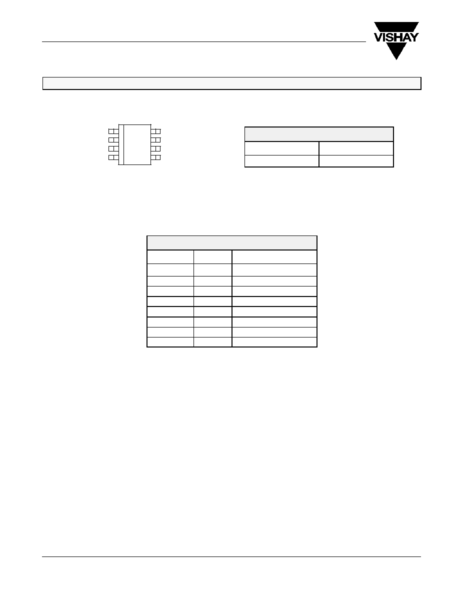
Top View
Narrow Body
RX
L
RX
K
TX
V
BAT
K
GND
SO Package
V
DD
L
Si9243AEY
Vishay Siliconix
www.vishay.com
4
Document Number: 70788
S-02936--Rev. D, 22-Jan-01
PIN CONFIGURATION
ORDERING INFORMATION
Part Number
Temperature Range
Si9243AEY
≠40 to 125
_
C
PIN DESCRIPTION
Pin Number
Symbol
Description
1
RX
K
K Receiver, Output
2
RX
L
L Receiver, Output
3
V
DD
Positive Power Supply
4
TX
Transmit, Input
5
GND
Ground Connection
6
K
K Transmit/Receive, Bidirectional
7
V
BAT
Battery Power Supply
8
L
L Transmit, Input
FUNCTIONAL DESCRIPTION
The Si9243AEY can be either in transmit or receive mode and
it contains over temperature, and short circuit V
BAT
fault
detection circuits.
The voltage on the K and L pins are internally compared to
V
BAT/2
. If the voltage on the K or L pin is less than V
BAT/2
then
RX
K
or RX
L
output will be "low." If the voltage on the K or L pin
is greater than V
BAT/2
then RX
K
or RX
L
output will be "high.
In order to be in transmit mode, TX must be set "low." The TX
signal is then internally inverted and turns the MOSFET on,
causing the K pin to be "low." In transmit mode, the processor
monitors the RX
K
and TX. When the two mirror each other
there is no fault. In the event of over temperature, or short
circuit to V
BAT
, the Si9243AEY will turn off the K output to
protect the IC. The K pin will stay in high impedance and RX
K
will follow the K pin. The fault will be reset when TX is toggled
high. RX
K
, RX
L
and TX pins have internal pull up resistor to
V
DD
while K and L pins have internal pull down resistors. When
any one of the TX, V
BAT
or GND pins is open the K output is off.
When the TX pin is set "high" the Si9243AEY is in receive
mode and the internal MOSFET is turned off. RX
L
and RX
K
outputs will follow L and K inputs respectively.
Si9243AEY
Vishay Siliconix
Document Number: 70788
S-02936--Rev. D, 22-Jan-01
www.vishay.com
5
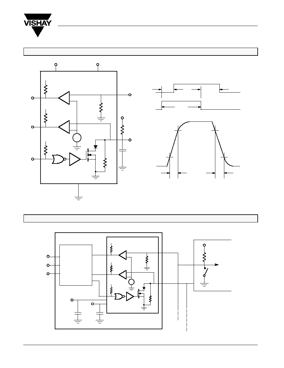
TEST CIRCUIT AND TIMING DIAGRAMS (TRANSMIT ONLY)
t
d(off)
V
K
, V
L
V
BAT
V
DD
GND
K
TX
Si9243AEY
V
BAT
R
L
C
L
80%
80%
20%
20%
t
r
t
f
≠
+
V
≠
+
RX
K
TX
min
t
d(on)
V
BAT
R
L
= 510
W
, C
L
= 10 nF, V
BAT
= 6 V to 18 V
R
L
= 1 k
W
, C
L
= 4.7 nF, V
BAT
= 16 V to 36 V
≠
+
RX
L
RX
K
L
TX
V
DD
V
DD
V
DD
APPLICATION CIRCUIT
V
B
Microcontroller
ECU
I/Os
ECU = Electronic Control Unit
L-Line
Diagnostic Tester
510
W
0.4
W
K-Line
Bus
V
DD
V
BAT
C1
0.1
m
F
C1
0.1
m
F
50 V
Si9243AEY
≠
+
V
≠
+
≠
+
V
DD
V
DD
V
DD