 | –≠–ª–µ–∫—Ç—Ä–æ–Ω–Ω—ã–π –∫–æ–º–ø–æ–Ω–µ–Ω—Ç: SI9434DY | –°–∫–∞—á–∞—Ç—å:  PDF PDF  ZIP ZIP |
Si9434DY
Siliconix
Vishay-Siliconix, 2201 Laurelwood Road, Santa Clara, CA 95054
S
Phone (408)988-8000
S
FaxBack (408)970-5600
S
www.siliconix.com
S-56981--Rev. H, 15-Jun-98 Siliconix was formerly a division of TEMIC Semiconductors
1
P-Channel Enhancement-Mode MOSFET
PRODUCT SUMMARY
V
DS
(V)
R
DS(ON)
(W)
I
D
(A)
≠20
0.040 @ V
GS
= ≠4.5 V
"
6.4
≠20
0.060 @ V
GS
= ≠2.5 V
"
5.1
Recommended upgrade: Si9424DY
S
D
S
D
S
D
G
D
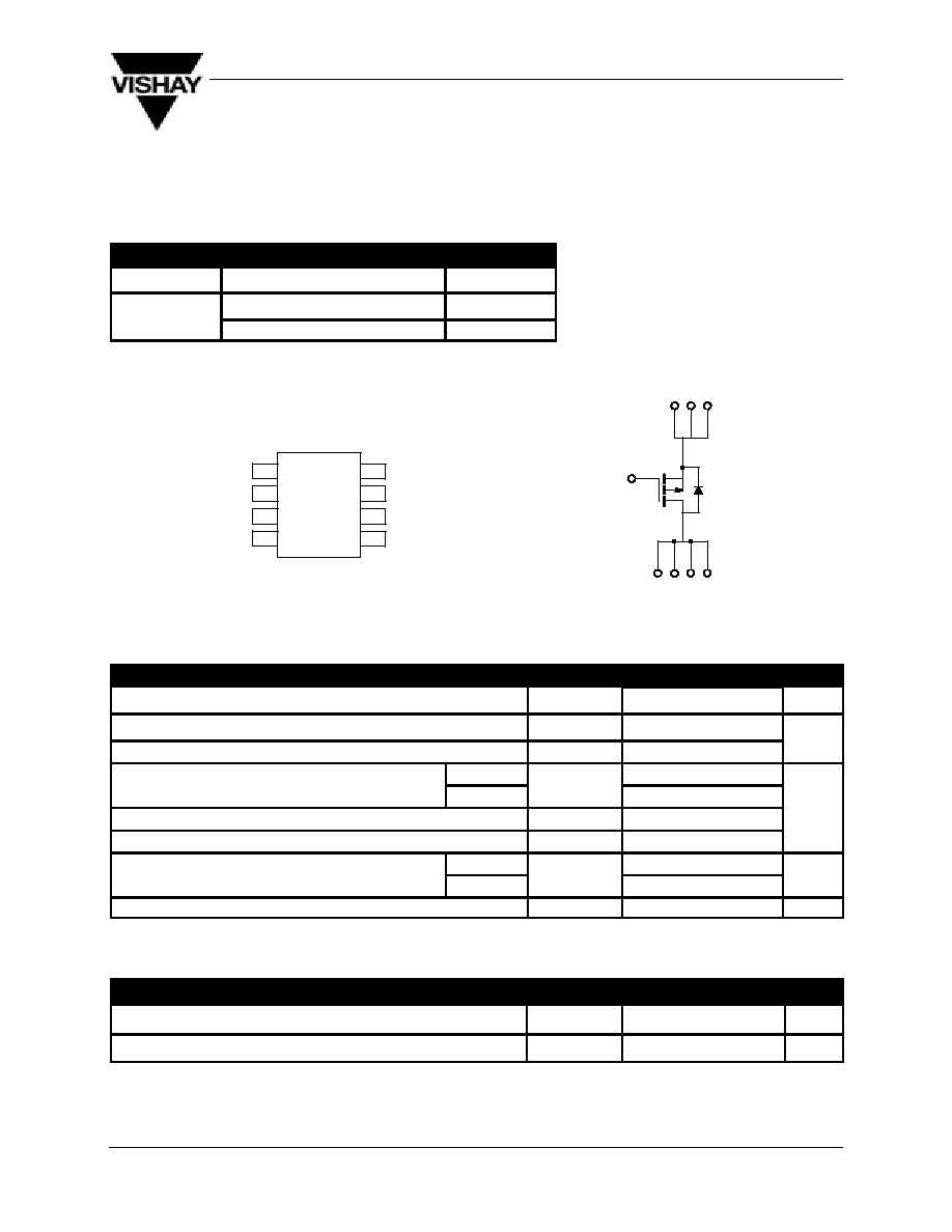
SO-8
5
6
7
8
Top View
2
3
4
1
S S S
G
D
D
D
D
P-Channel MOSFET
ABSOLUTE MAXIMUM RATINGS (T
A
= 25_C UNLESS OTHERWISE NOTED)
PARAMETER
SYMBOL
LIMIT
UNIT
Drain-Source Voltage
V
DS
≠20
V
Gate-Source Voltage
V
GS
"
8
V
Continuous Drain Current (T
J
= 150
_
C)
A
T
A
= 25
_
C
I
D
"
6.4
Continuous Drain Current
(T
J
= 150 C)
A
T
A
= 70
_
C
I
D
"
5.1
A
Pulsed Drain Current
I
DM
"
10
A
Continuous Source Current (Diode Conduction)
A
I
S
≠2.5
Maximum Power Dissipation
A
T
A
= 25
_
C
P
D
2.5
W
Maximum Power Dissi ation
A
T
A
= 70
_
C
P
D
1.6
W
Operating Junction and Storage Temperature Range
T
J
, T
stg
≠55 to 150
_
C
THERMAL RESISTANCE RATINGS
PARAMETER
SYMBOL
LIMIT
UNIT
Maximum Junction-to-Ambient
A
R
thJA
50
_
C/W
Notes
A.
Surface Mounted on FR4 Board, t
v
10 sec.
Updates to this data sheet may be obtained via facsimile by calling Siliconix FaxBack, 1-408-970-5600. Please request FaxBack document #70147.
A SPICE Model data sheet is available for this product (FaxBack document #70528).
Siliconix
Si9434DY
Vishay-Siliconix, 2201 Laurelwood Road, Santa Clara, CA 95054
S
Phone (408)988-8000
S
FaxBack (408)970-5600
S
www.siliconix.com
S-56981--Rev. H, 15-Jun-98 Siliconix was formerly a division of TEMIC Semiconductors
2
SPECIFICATIONS (T
J
=25_C UNLESS OTHERWISE NOTED)
PARAMETER
SYMBOL
TEST CONDITION
MIN
TYP
MAX
UNIT
STATIC
Gate Threshold Voltage
V
GS(th)
V
DS
= V
GS
, I
D
= ≠250
m
A
≠0.6
V
Gate-Body Leakage
I
GSS
V
DS
= 0 V, V
GS
=
"
8 V
"
100
nA
Zero Gate Voltage Drain Current
I
DSS
V
DS
= ≠16 V, V
GS
= 0 V
≠1
m
A
Zero Gate Voltage Drain Current
I
DSS
V
DS
= ≠16 V, V
GS
= 0 V, T
J
= 70
_
C
≠5
m
A
On-State Drain Current
A
I
D(on)
V
DS
v
≠5 V, V
GS
= ≠4.5 V
≠10
A
On-State Drain Current
A
I
D(on)
V
DS
v
≠5 V, V
GS
= ≠2.5 V
≠5
A
Drain-Source On-State Resistance
A
r
DS(on)
V
GS
= ≠4.5 V, I
D
= ≠6.4 A
0.031
0.040
W
Drain-Source On-State Resistance
A
r
DS(on)
V
GS
= ≠2.5 V, I
D
= ≠5.1 A
0.045
0.060
W
Forward Transconductance
A
g
fs
V
DS
= ≠9 V, I
D
= ≠6.4 A
14
S
Diode Forward Voltage
A
V
SD
I
S
= ≠2.5 A, V
GS
= 0 V
≠0.9
≠1.2
V
Dynamic
B
Total Gate Charge
Q
g
30
50
Gate-Source Charge
Q
gs
V
DS
= ≠10 V,
V
GS
= ≠4.5 V, I
D
= ≠6.4 A
5
nC
Gate-Drain Charge
Q
gd
9
Turn-On Delay Time
t
d(on)
25
50
Rise Time
t
r
V
DD
= ≠10 V, R
L
= 6
W
42
80
Turn-Off Delay Time
t
d(off)
DD
L
I
D
^
≠1 A, V
GEN
= ≠4.5 V, R
G
= 6
W
160
200
ns
Fall Time
t
f
75
120
Source-Drain Reverse Recovery Time
t
rr
I
F
= ≠2.5 A, di/dt = 100 A/
m
s
50
100
Notes
A.
Pulse test; pulse width
v
300
m
s, duty cycle
v
2%.
B.
Guaranteed by design, not subject to production testing.
Si9434DY
Siliconix
Vishay-Siliconix, 2201 Laurelwood Road, Santa Clara, CA 95054
S
Phone (408)988-8000
S
FaxBack (408)970-5600
S
www.siliconix.com
S-56981--Rev. H, 15-Jun-98 Siliconix was formerly a division of TEMIC Semiconductors
3
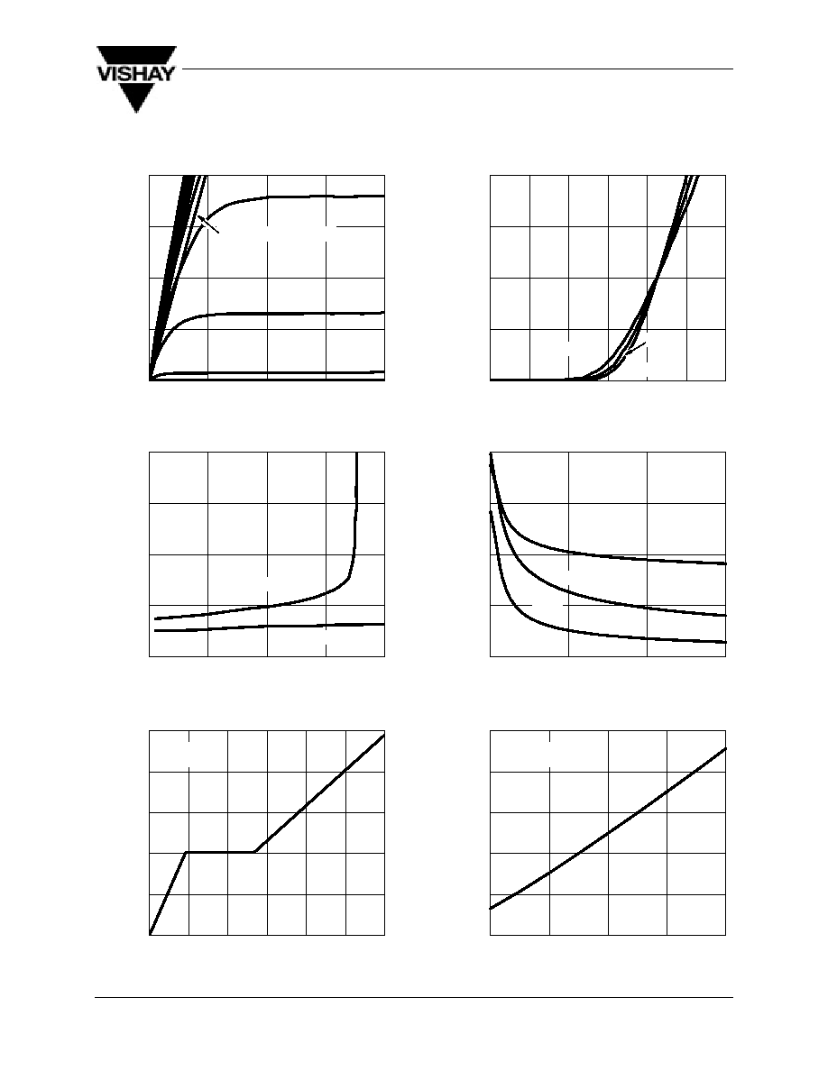
Typical Characteristics (25
_
C Unless Otherwise Noted)
0
5
10
15
20
0
1
2
3
4
0
1
2
3
4
5
0
5
10
15
20
25
30
0.6
0.8
1.0
1.2
1.4
1.6
≠50
0
50
100
150
0
0.05
0.10
0.15
0.20
0
5
10
15
20
0
1000
2000
3000
4000
0
4
8
12
0
5
10
15
20
0
0.5
1.0
1.5
2.0
2.5
3.0
Output Characteristics
Transfer Characteristics
Gate Charge
On Resistance vs. Drain Current
V
DS
≠ Drain-to-Source Voltage (V)
≠ Drain Current (A)
I
D
V
GS
= 5, 4.5, 4, 3.5, 3 V
2 V
V
GS
≠ Gate-to-Source Voltage (V)
≠ Drain Current (A)
I
D
T
C
= 125
_
C
≠55
_
C
≠ Gate-to-Source V
oltage
(V)
Q
g
≠ Total Gate Charge (nC)
V
DS
≠ Drain-to-Source Voltage (V)
C ≠ Capacitance (pF)
V
GS
C
rss
C
oss
C
iss
V
DS
= 10 V
I
D
= 6.4 A
I
D
≠ Drain Current (A)
Capacitance
On Resistance vs. Junction Temperature
V
GS
= 4.5 V
I
D
= 6.4 A
T
J
≠ Junction Temperature (
_
C)
V
GS
= 2.5 V
V
GS
= 4.5 V
25
_
C
2.5 V
1.5 V
≠ On-Resistance (
r
DS(on)
W
)
(Normalized)
≠ On-Resistance (
r
DS(on)
W
)
Siliconix
Si9434DY
Vishay-Siliconix, 2201 Laurelwood Road, Santa Clara, CA 95054
S
Phone (408)988-8000
S
FaxBack (408)970-5600
S
www.siliconix.com
S-56981--Rev. H, 15-Jun-98 Siliconix was formerly a division of TEMIC Semiconductors
4
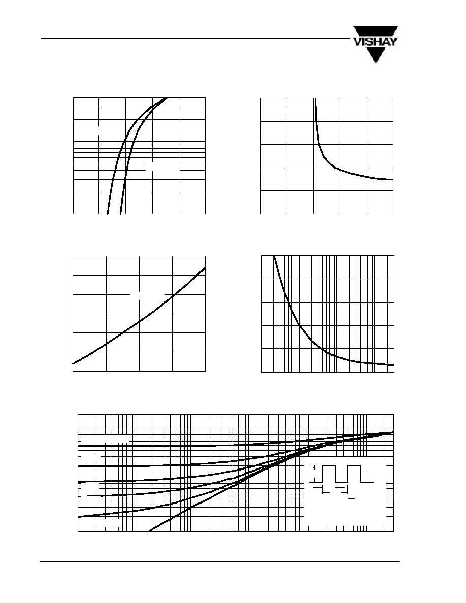
Typical Characteristics (25
_
C Unless Otherwise Noted)
0
0.4
0.8
1.2
1.6
2.0
Power (W)
0
0.1
40
50
10
20
30
1
10
30
Single Pulse Power
Time (sec)
0.01
0
0.020
0.040
0.060
0.080
0.100
0
1
2
3
4
5
Source Drain Diode Forward Voltage
On Resistance vs. Gate to Source
Voltage
Threshold Voltage
Normalized Thermal Transient Impedance, Junction to Ambient
Square Wave Pulse Duration (sec)
2
1
0.1
0.01
10
≠4
10
≠3
10
≠2
10
≠1
1
10
Normalized Ef
fective
T
ransient
Thermal Impedance
30
0.2
0.1
0.05
0.02
Single Pulse
Duty Cycle = 0.5
V
SD
≠ Source-to-Drain Voltage (V)
V
GS
≠ Gate-to-Source Voltage (V)
≠ Source Current (A)
I
S
T
J
≠ Temperature (
_
C)
V
ariance (V)
V
GS(th)
≠0.20
≠0.10
0.00
0.10
0.20
0.30
0.40
≠50
0
50
100
150
T
J
= 150
_
C
I
D
=
6.4
A
I
D
= 250
m
A
40
1
10
1. Duty Cycle, D =
2. Per Unit Base = R
thJA
= 50
_
C/W
3. T
JM
≠ T
A
= P
DM
Z
thJA
(t)
t
1
t
2
t
1
t
2
Notes:
4. Surface Mounted
P
DM
T
J
= 25
_
C
≠ On-Resistance (
r
DS(on)
W
)