Si9910
Vishay Siliconix
Document Number: 70009
S-40707--Rev. G, 19-Apr-04
www.vishay.com
1
Adaptive Power MOSFET Driver
1
FEATURES
D dv/dt and di/dt Control
D Undervoltage Protection
D Short-Circuit Protection
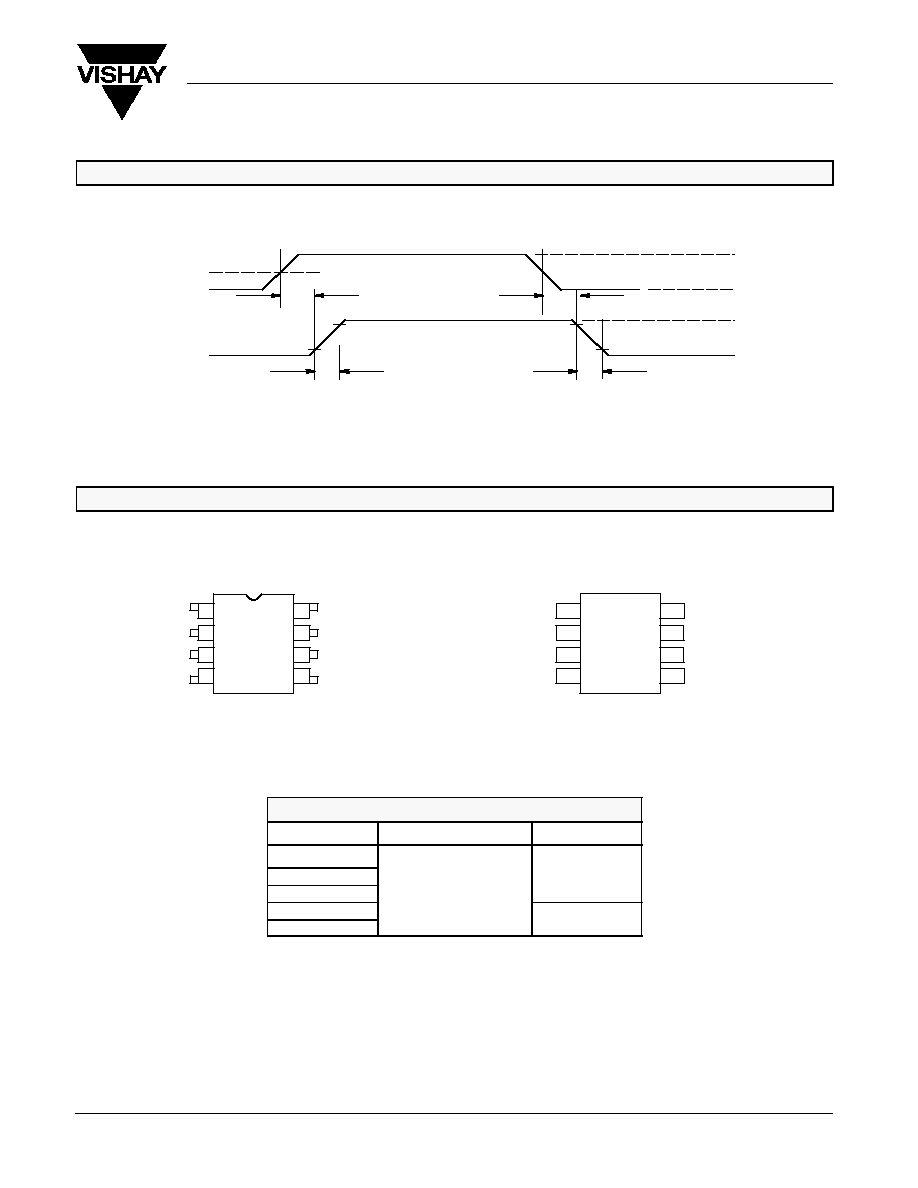
D t
rr
Shoot-Through Current Limiting
D Low Quiescent Current
D CMOS Compatible Inputs
D Compatible with Wide Range of MOSFET Devices
D Bootstrap and Charge Pump Compatible
(High-Side Drive)
DESCRIPTION
The Si9910 Power MOSFET driver provides optimized gate
drive signals, protection circuitry and logic level interface. Very
low quiescent current is provided by a CMOS buffer and a
high-current emitter-follower output stage. This efficiency
allows operation in high-voltage bridge applications with
"bootstrap" or "charge-pump" floating power supply
techniques.
The non-inverting output configuration minimizes current
drain for an n-channel "on" state. The logic input is internally
diode clamped to allow simple pull-down in high-side drives.
Fault protection circuitry senses an undervoltage or output
short-circuit condition and disables the power MOSFET.
Addition of one external resistor limits maximum di/dt of the
external Power MOSFET. A fast feedback circuit may be used
to limit shoot-through current during t
rr
(diode reverse recovery
time) in a bridge configuration.
The Si9910 is available in 8-pin plastic DIP and SOIC
packages, and are specified over the industrial, D suffix (-40
to 85_C) temperature range. In SOIC-8 packaging both
standard and lead (Pb)-free options are available.
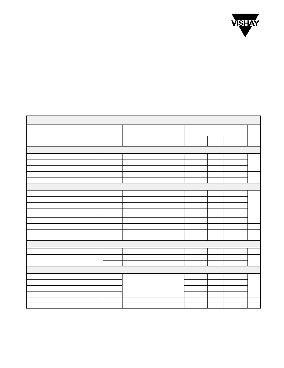
FUNCTIONAL BLOCK DIAGRAM
DRAIN
PULL-UP
PULL-DOWN
C1
* Typical Values
V
DD
V
SS
R2
*250 W
R3
*100 kW
V
DS
Undervoltage/
Overcurrent
Protection
*2 to 5 pF
I
SENSE
INPUT
R1
*0.1 W
2-ms
Delay
1. Patent Number 484116.
Si9910
Vishay Siliconix
www.vishay.com
2
Document Number: 70009
S-40707--Rev. G, 19-Apr-04
ABSOLUTE MAXIMUM RATINGS
Voltages Referenced to V
SS
Pin
V
DD
Supply Range
-0.3 V to 18 V
. . . . . . . . . . . . . . . . . . . . . . . . . . . . . . . . . . .
Pin 1, 4, 5, 7, 8
-0.3 V to V
DD
+ 0.3 V
. . . . . . . . . . . . . . . . . . . . . . . . . . . . . . . .
Pin 2
-0.7 V to V
DD
+ 0.3 V
. . . . . . . . . . . . . . . . . . . . . . . . . . . . . . . . . . . . . . . . .
Input Current
"20 mA
. . . . . . . . . . . . . . . . . . . . . . . . . . . . . . . . . . . . . . . . . . . . .
Peak Current (I
pk
)
1 A
. . . . . . . . . . . . . . . . . . . . . . . . . . . . . . . . . . . . . . . . . . . . . .
Storage Temperature
-65 to 150_C
. . . . . . . . . . . . . . . . . . . . . . . . . . . . . . . . . .
Operating Temperature
-40 to 85_C
. . . . . . . . . . . . . . . . . . . . . . . . . . . . . . . . .
Junction Temperature (T
J
)
150_C
. . . . . . . . . . . . . . . . . . . . . . . . . . . . . . . . . . . .
Power Dissipation (Package)
a
8-Pin SOIC (Y Suffix)
b
700 mW
. . . . . . . . . . . . . . . . . . . . . . . . . . . . . . . . . . . . .
8-Pin Plastic DIP (J Suffix)
b
700 mW
. . . . . . . . . . . . . . . . . . . . . . . . . . . . . . . . .
Notes
a.
Device mounted with all leads soldered or welded to PC board.
b.
Derate 5.6 mW/_C above 25_C.
SPECIFICATIONS
a
Test Conditions
Unless Otherwise Specified
Limits
Parameter
Symbol
Unless Otherwise Specified
V
DD
10.8 V to 16.5 V
T
A
= OperatingTemperature Range
Min
c
Typ
b
Max
c
Unit
Input
High Level Input Voltage
V
IH
0.70 x V
DD
7.4
Low Level Input Voltage
V
IL
6.0
0.35 x V
DD
V
Input Voltage Hysteresis
V
h
0.90
2.0
3.0
High Level Input Current
I
IH
V
IN
= V
DD
"1
mA
Low Level Input Current
I
IL
V
IN
= 0 V
"1
mA
Output
High Level Output Voltage
V
OH
I
OH
= -200 mA
V
DD
-3
10.7
Low Level Output Voltage
V
OL
I
OL
= 200 mA
1.3
3
Undervoltage Lockout
V
UVLO
8.3
9.2
10.6
V
I
SENSE
Pin Threshold
V
TH
Max I
S
= 2 mA, Input High
100 mV Change on Drain
0.5
0.66
0.8
V
Voltage Drain-Source Maximum
V
DS
Input High
8.3
9.1
10.2
Input Current for V
DS
Input
I
VDS
12
20.0
mA
Peak Output Source Current
I
OS+
1
A
Peak Output Sink Current
I
OS-
-1
Supply
Supply Range
V
DD
10.8
16.5
V
Supply Current
I
DD1
Output High, No Load
0.1
1
mA
Supply Current
I
DD2
Output Low, No Load
100
500
mA
Dynamic
Propagation Delay Time Low to High Level
t
PLH
120
Propagation Delay Time High to Low Level
t
PHL
C
L
= 2000 pF
135
ns
Rise Time
t
r
C
L
= 2000 pF
50
ns
Fall Time
t
f
35
Overcurrent Sense Delay (V
DS
)
t
DS
1
mS
Input Capacitance
C
in
5
pF
Notes
a.
Refer to PROCESS OPTION FLOWCHART for additional information.
b.
Typical values are for DESIGN AID ONLY, not guaranteed nor subject to production testing.
c.
The algebraic convention whereby the most negative value is a minimum and the most positive a maximum.

Si9910
Vishay Siliconix
www.vishay.com
4
Document Number: 70009
S-40707--Rev. G, 19-Apr-04
PIN DESCRIPTION
Pin 1: V
DS
Pin 1 or V
DS
is a sense input for the maximum source-drain
voltage limit. Two microseconds after a high transition on input
pin 2, an internal timer enables the V
DS(max)
sense circuitry. A
catastrophic overcurrent condition, excessive on-resistance,
or insufficient gate-drive voltage can be sensed by limiting
the maximum voltage drop across the power MOSFET. An
external resistor (R3) is required to protect pin 1 from
overvoltage during the MOSFET "off" condition. Exceeding
V
DS(max)
latches the Si9910 "off." Drive is re-enabled on the
next positive- going input on pin 2. If pin 1 is not used, it must
be connected to pin 6 (V
SS
).
Pin 2: INPUT
A non-inverting, Schmidt trigger input controls the state of the
MOSFET gate-drive outputs and enables the protection logic.
When the input is low (v V
IL
), V
DD
is monitored for an
undervoltage condition (insufficiently charged bootstrap
capacitor). If an undervoltage (v V
DD(min)
) condition exists,
the driver will ignore a turn-on input signal. An undervoltage
(v V
DD(min)
) condition during an "on" state will not be sensed.
Pin 3: V
DD
V
DD
supplies power for the driver's internal circuitry and
charging current for the power MOSFET's gate capacitance.
The Si9910 minimizes the internal I
DD
in the
"on" state
(gate-drive outputs high) allowing a "floating" power supply to
be provided by charge pump or bootstrap techniques.
Pin 4: DRAIN
Drain is an analog input to the internal dv/dt limiting circuitry.
An external capacitor (C1) must be used to protect the input
from exposure to the high-voltage ("off" state) drain and to set
the power MOSFET's maximum rate of dv/dt. If dv/dt feedback
is not used, pin 4 must be left open.
Pin 5: I
SENSE
I
SENSE
in combination with an external resistor (R
1)
protects the power MOSFET from potentially catastrophic
peak currents. I
SENSE
is an analog feedback that limits current
during the power MOSFET's transition to an "on" state. It is
intended to protect power MOSFETs (in a half-bridge
arrangement) from "shoot-through" current, resulting from
excess di/dt and t
rr
of flyback diodes or from logic timing
overlap. An 0.8-V drop across (R1) should indicate a current
level that is approximately four times the maximum allowable
load current. When the I
SENSE
input is not used, it should be
tied to pin 6 (V
SS
).
Pin 6: V
SS
V
SS
is the driver's ground return pin. The applications diagram
illustrates the connection of V
SS
for source-referenced
"floating" applications (half-bridge, high-side) and
ground-referenced applications (half-bridge, low-side).
Pin 7: PULL-DOWN
Pin 8: PULL-UP
Pull-up and pull-down outputs collectively provide the power
MOSFET gate with charging and discharging currents. Turn
"on" or "off" di/dt can be limited by adding resistance (R
2
) in
series with the appropriate output.
APPLICATIONS
"Floating" High-Side Drive Applications
As demonstrated in Figure 1, the Si9910 is intended for use
as both a ground-referenced gate driver and as a "high-side"
or source-referenced gate driver in half-bridge applications.
Several features of the Si9910 permit its use in half-bridge
high-side drive applications.
A simple and inexpensive method of isolating a floating supply
to power the Si9910 in high-side driver applications had to be
provided. Therefore, the Si9910 was designed to be
compatible with two of the most commonly used floating
supply techniques: the bootstrap and the charge pump. Both
of these techniques have limitations when used alone. A
properly designed bootstrap circuit can provide
low-impedance drive which minimizes transition losses and
the charge pump circuit provides static operation.
The Si9910 is configured to take advantage of either floating
supply technique if the application is not sensitive to their
particular limitations, or both techniques if switching losses
must be minimized and static operation is necessary. The
schematic above illustrates both the charge pump and
bootstrap circuits used in conjunction with an Si9910 in a
high-side driver application.
Input signal level shifting is accomplished with a passive
pull-up (R4) and n-channel MOSFET (Q2) for pull-down in
applications below 500 V. Total node capacitance defines the
value of R4 needed to guarantee an input transition rate which
safely exceeds the maximum dv/dt rate of the output
half-bridge. Using level-shift devices with higher current
capabilities may necessitate the addition of current-limiting
components such as R5.
Bootstrap Undervoltage Lockout
When using a bootstrap capacitor as a high-side floating
supply, care must be taken to ensure time is available to
recharge the bootstrap capacitor prior to turn-on of the
high-side MOSFET. As a catastrophic protection against
abnormal conditions such as start-up, loss of power, etc., an
internal voltage monitor has been included which monitors the
bootstrap voltage when the Si9910 is in the low state. The
Si9910 will not respond to a high input signal until the voltage
on the bootstrap capacitor is sufficient to fully enhance the
power MOSFET gate. For more details, please refer to
Application Note AN705.