V
DD
OUTPUT
A
B
IN
A
IN
B
GND
S
A
Shoot-Through
Protection Logic
S
B
GND
SO-8
5
6
7
8
Top View
2
3
4
1
S
A
OUT
A
V
DD
IN
A
IN
B
S
B
OUT
B
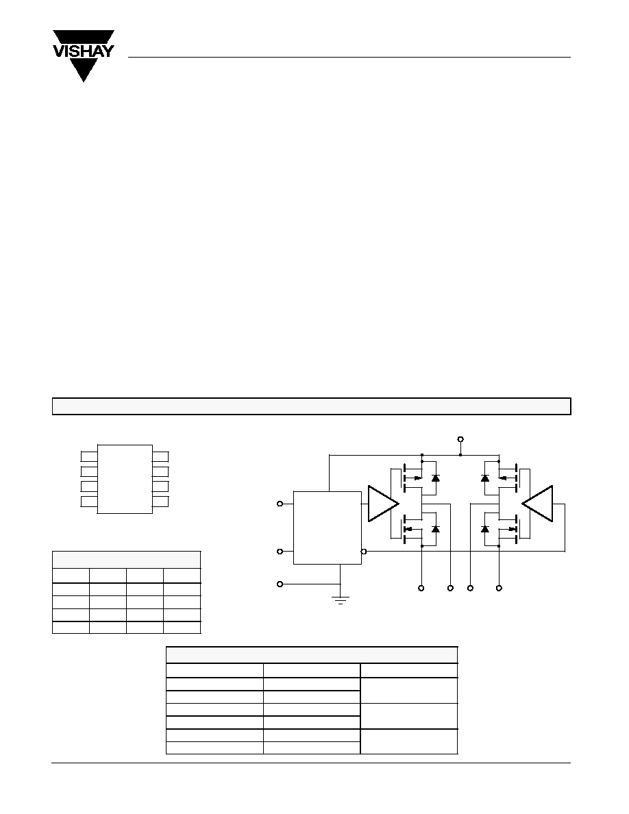
Si9986
(3)
(7)
(6)
(2)
(1)
(8)
(5)
(4)
Si9986
Vishay Siliconix
Document Number: 70007
S-40131--Rev. E, 16-Feb-04
www.vishay.com
1
Buffered H-Bridge
FEATURES
APPLICATIONS
D 1.0-A H-Bridge
D 200-kHz Switching Rate
D Shoot-Through Limited
D TTL Compatible Inputs
D 3.8- to 13.2-V Operating Range
D Surface Mount Packaging
D VCM Driver
D Brushed Motor Driver
D Stepper Motor Driver
D Power Converter
D Optical Disk Drives
D Power Supplies
D High Performance Servo
DESCRIPTION
The Si9986 is an integrated, buffered H-bridge with TTL
compatible inputs and the capability of delivering a continuous
1.0 A @ V
DD
= 12 V (room temperature) at switching rates up to
200 kHz. Internal logic prevents the upper and lower outputs of
either half-bridge from being turned on simultaneously. Unique
input codes allow both outputs to be forced low (for braking) or
forced to a high impedance level.
The Si9986 is available in both standard and lead (Pb)-free,
8-pin SOIC packages, specified to operate over a voltage
range of 3.8 V to 13.2 V, and the commercial temperature
range of 0 to 70_C (C suffix) and the industrial temperature
range of -40 to 85_C (D suffix).
FUNCTIONAL BLOCK DIAGRAM, PIN CONFIGURATION AND TRUTH TABLE
TRUTH TABLE
IN
A
IN
B
OUT
A
OUT
B
1
0
1
0
0
1
0
1
0
0
0
0
1
1
HiZ
HiZ
ORDERING INFORMATION
Part Number
Temperature Range
Package
Si9986CY-T1
0 to 70_C
Tape and Reel
Si9986DY-T1
-40 to 85_C
Tape and Reel
Si9986CY-T1--E3
0 to 70_C
Lead Free Tape and Reel
Si9986DY-T1--E3
-40 to 85_C
Lead Free Tape and Reel
Si9986CY
0 to 70_C
Bulk (tubes)
Si9986DY
-40 to 85_C
Bulk (tubes)

Si9986
Vishay Siliconix
www.vishay.com
2
Document Number: 70007
S-40131--Rev. E, 16-Feb-04
ABSOLUTE MAXIMUM RATINGS
a
Voltage on any pin with respect to ground
-0.3 V to V
DD
+0.3 V
. . . . . . . . . . .
Voltage on pins 5, 8 with respect to GND
-1 V to V
DD
+1 V
. . . . . . . . . . . . . .
Voltage on pins 1, 4
-0.3 V to GND +1 V
. . . . . . . . . . . . . . . . . . . . . . . . . . . . .
Peak Output Current
1.5 A
. . . . . . . . . . . . . . . . . . . . . . . . . . . . . . . . . . . . . . . . .
Storage Temperature
-65 to 150_C
. . . . . . . . . . . . . . . . . . . . . . . . . . . . . . . . . .
Maximum Junction Temperature (T
J
)
150_C
. . . . . . . . . . . . . . . . . . . . . . . . . . .
Maximum V
DD
15 V
. . . . . . . . . . . . . . . . . . . . . . . . . . . . . . . . . . . . . . . . . . . . . .
Power Dissipation
b
1
W
. . . . . . . . . . . . . . . . . . . . . . . . . . . . . . . . . . . . . . . . . . .
q
JA
100_C/W
. . . . . . . . . . . . . . . . . . . . . . . . . . . . . . . . . . . . . . . . . . . . . . . . . . . . .
Operating Temperature Range
Si9986CY
0 to 70_C
. . . . . . . . . . . . . . . . . . . . . . . . . . . . . . . . . . . . . . . . . . . . . .
Si9986DY
-40 to 85_C
. . . . . . . . . . . . . . . . . . . . . . . . . . . . . . . . . . . . . . . . . . . .
Notes
a.
Device mounted with all leads soldered or welded to PC board.
b.
Derate 10 mW/_C above 25_C.
RECOMMENDED OPERATING RANGE
V
DD
3.8 V to 13.2 V
. . . . . . . . . . . . . . . . . . . . . . . . . . . . . . . . . . . . . . . . . . . . . . . .
Maximum Junction Temperature (T
J
)
125_C
. . . . . . . . . . . . . . . . . . . . . . . . . . .
SPECIFICATIONS
Test Conditions
Unless Otherwise Specified
V
DD
= 3 8 to 13 2 V
Limits
C Suffix, 0 to 70_C
D Suffix, -40 to 85_C
Parameter
Symbol
V
DD
= 3.8 to 13.2 V
S
A
@ GND, S
B
@ GND
Min
a
Typ
b
Max
a
Unit
Input
Input Voltage High
V
INH
2
V
Input Voltage Low
V
INL
1
V
Input Current with Input Voltage High
I
INH
V
IN
= 2 V
1
mA
Input Current with Input Voltage Low
I
INL
V
IN
= 0 V
-1
mA
Output
I
OUT
= -500 mA
V
DD
= 10.8 V
10.5
10.7
Output Voltage High
V
OUTH
I
OUT
= -500 mA
V
DD
= 4.5 V
4.1
4.3
I
OUT
= -300 mA, V
DD
= 3.8 V
3.4
3.7
V
I
OUT
= 500 mA
V
DD
= 10.8 V
0.2
0.3
V
Output Voltage Low
V
OUTL
I
OUT
= 500 mA
V
DD
= 4.5 V
0.2
0.4
p
g
OUTL
I
OUT
= 300 mA, V
DD
= 3.8 V
0.1
0.4
Output Leakage Current High
I
OLH
IN
A
= IN
B
w 2 V, V
OUT
= V
DD
= 13.2 V
-10
0
mA
Output Leakage Current Low
I
OLL
V
OUT
= 0, V
DD
= 13.2 V
0
10
mA
Output V Clamp High
V
CLH
IN
A
= IN
B
w 2 V
I
OUT
= 100 mA
V
DD
+0.7
V
Output V Clamp Low
V
CLL
IN
A
= IN
B
w 2 V
I
OUT
= -100 mA
-0.7
V
Supply
V
DD
Supply Current
I
DD
IN = 100 kHz, V
DD
= 5 V
2
mA
V
DD
Supply Current
I
DD
IN
A
= IN
B
= 4.5 V, V
DD
= 5.5 V
300
mA
Dynamic
Propogation Delay Time
T
PLH
V
DD
= 5 V
300
nS
Propogation Delay Time
T
PHL
V
DD
= 5 V
100
nS
Notes
a.
The algebraic convention whereby the most negative value is a minimum and the most positive a maximum, is used in this data sheet.
b.
Typical values are for DESIGN AID ONLY, not guaranteed nor subject to production testing.
Si9986
Vishay Siliconix
Document Number: 70007
S-40131--Rev. E, 16-Feb-04
www.vishay.com
3
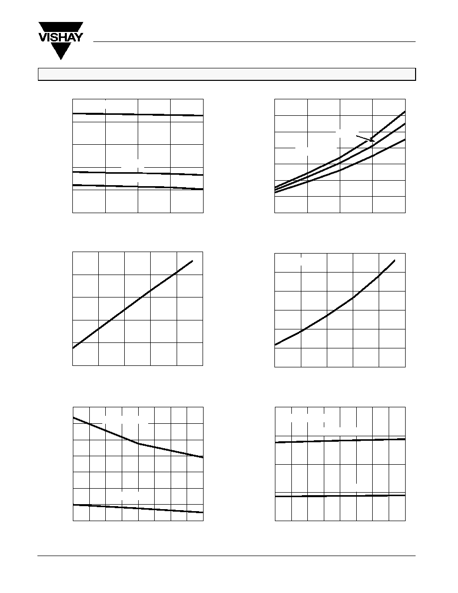
TYPICAL CHARACTERISTICS (25_C UNLESS NOTED)
0
2
4
6
8
-35
-20
-5
10
25
40
55
70
85
(mA)
I DD
Supply Current vs. Temperature
Temperature (_C)
V
DD
= 13.2 V
5.5 V
f = 100 kHz
-
Standby (
I DD
A)
m
60
80
100
120
140
160
180
200
-35
-20
-5
10
25
40
55
70
85
Supply Current vs. Temperature
Temperature (_C)
V
DD
= 13.2 V
5.5 V
0
1
2
3
4
5
6
4
6
8
10
12
14
Supply Current vs. Supply Voltage
(mA)
I DD
V
DD
- Supply Voltage (V)
f = 100 kHz
40
60
80
100
120
140
4
6
8
10
12
14
Supply Current vs. Supply Voltage
V
DD
- Supply Voltage (V)
0
100
200
300
400
500
600
700
0.50
0.75
1.00
1.25
1.50
0
3
6
9
12
15
0.50
0.75
1.00
1.25
1.50
Output High Voltage vs. Output Current
Output Low Voltage vs. Output Current
(V)
V
OUTH
Output Current (A)
Output Current (A)
(mV)
V
OUTL
V
DD
= 13.2 V
V
DD
= 3.8 V
5.5 V
3.8 V
5.5 V
13.2 V
-
Standby (
I DD
A)
m
