SiP2800/01/02/03/04/05
Vishay Siliconix
New Product
Document Number: 72660
S-41623--Rev.C, 30-Aug-04
www.vishay.com
1
Low Power Consumption Current Mode Controller
FEATURES
D
Pin-for-Pin Compatible with UCC280X Controllers
D
Enhanced Performance UC284X for New Designs
D
100-
m
A Typical Start-Up Current
D
500-
m
A Typical Operating Current
D
Internal Soft Start at Power-On and After Fault
D
100-ns Internal Leading Edge Blanking
APPLICATIONS
D
Efficiency-Enhanced DC/DC Converter Modules
D
Low Quiescent Current Standby Power Supplies
D
Offline (AC/DC) Power Supplies
D
Universal Input Power Supplies
D
Buck, Boost, and Buck-Boost Converters
DESCRIPTION
The SiP280X family includes six high-speed, low power
consumption, BiCMOS Current Mode Controllers. These
integrated circuits contain all of the control and drive functions
required for off-line and dc-to-dc current-mode switching
power supplies. Their advanced architecture enables the
implementation of full-featured designs with minimal external
parts count.
The SiP280X family controllers are available in both standard
and lead (Pb)-free, SO-8 and TSSOP-8 packages, and are
rated for operation over the industrial temperature range of
--40 to 85
_
C.
Part Number
Maximum
Duty Cycle
Reference
Voltage
Turn-On
Threshold
Turn-Off
Threshold
SiP2800
100%
5 V
7.2 V
6.9 V
SiP2801
50%
5 V
9.4 V
7.4 V
SiP2802
100%
5 V
12.5 V
8.3 V
SiP2803
100%
4 V
4.1 V
3.6 V
SiP2804
50%
5 V
12.5 V
8.3 V
SiP2805
50%
4 V
4.1 V
3.6 V
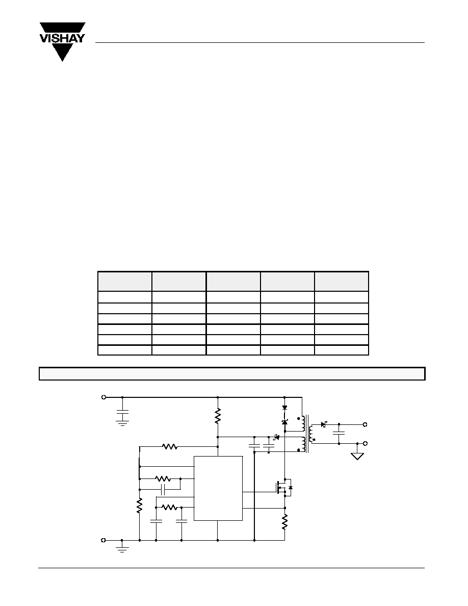
TYPICAL APPLICATION CIRCUIT
V
CC
REF
GND
RC
OUT
+48 V
GND
COMP
FB
CS
SiP2801
12 V/3 A
+
+
+
Flyback Converter for Point of Load Application
SiP2800/01/02/03/04/05
Vishay Siliconix
New Product
www.vishay.com
2
Document Number: 72660
S-41623--Rev.C, 30-Aug-04
ABSOLUTE MAXIMUM RATINGS
V
CC
12 V
. . . . . . . . . . . . . . . . . . . . . . . . . . . . . . . . . . . . . . . . . . . . . . . . . . . . . . . . .
FB, Comp, CS
--0.3 V to 6 V
. . . . . . . . . . . . . . . . . . . . . . . . . . . . . . . . . . . . . . . .
Power Disispation SO-8
1 W
. . . . . . . . . . . . . . . . . . . . . . . . . . . . . . . . . . . . . . . .
Power Disispation TSSOP-8
830 mW
. . . . . . . . . . . . . . . . . . . . . . . . . . . . . . . .
StorageTemperature
--55 to 150
_
C
. . . . . . . . . . . . . . . . . . . . . . . . . . . . . . . . . .
Currents are positive into, negative out of the specificed terminal.
Stresses beyond those listed under "Absolute Maximum Ratings" may cause permanent damage to the device. These are stress ratings only, and functional operation
of the device at these or any other conditions beyond those indicated in the operational sections of the specifications is not implied. Exposure to absolute maximum rating
conditions for extended periods may affect device reliability.
RECOMMENDED OPERATING RANGE
Input Voltage SiP2803/5
5 to 11 V
. . . . . . . . . . . . . . . . . . . . . . . . . . . . . . . . . . . .
Input Voltage SiP2800/1/2/4
6 to 11 V
. . . . . . . . . . . . . . . . . . . . . . . . . . . . . . . .
Operating Temperature Range
--40 to 85
_
C
. . . . . . . . . . . . . . . . . . . . . . . . . . .
SPECIFICATIONS
Test Conditions Unless Specified
Limits
Parameter
Symbol
V
CC
= 10 V, R
T
= 100 k
, C
T
= 330 pF
C
REF
= 0.1
m
F, --40
_
C < T
A
< 85
_
C
Min
a
Typ
b
Max
a
Unit
Reference
I
LOAD
= 0 2 mA T
A
= 25
�
C
SiP2800/1/2/4
4.925
5.000
5.075
Reference Voltage
V
REF
I
LOAD
= 0.2 mA, T
A
= 25
�
C
SiP2803/5
3.940
4.000
4.06
V
Reference Voltage
V
REF
SiP2800/1/2/4
4.88
5.00
5.10
V
SiP2803/5
3.90
4.00
4.08
Load Regulation
V
LOAD
0.2mA< I
LOAD
<5mA
10
30
mV
Line Regulation
V
Vcc=10 V to Clamp , T
A
= 25
�
C
1.9
mV/V
Line Regulation
V
LINE
Vcc=10 V to Clamp
2.5
mV/V
Noise
V
NOISE
10 Hz < f < 10 kHz T
25
�
C
130
m
V
Short Circuit Current
I
SC
10 Hz < f < 10 kHz, T
A
= 25
�
C
--5
--35
mA
Oscillator
Frequency
f
OSC
SiP2800/1/2/4
40
46
52
kHz
Frequency
f
OSC
SiP2803/5
26
31
36
kHz
Temperature Stability
2.5
%
Amplitude
V
P--P
2.25
2.40
2.55
V
Peak Voltage
V
P
2.45
V
Error Amplifier
Input Voltage
V
IN
COMP = 2.5 V
SiP2800/1/2/4
2.44
2.50
2.56
V
Input Voltage
V
IN
COMP = 2.0 V
SiP2803/5
1.95
2.00
2.05
V
Input Bias Current
I
BIAS1
--1
1
m
A
Open Loop Gain
A
V
60
80
dB
COMP Sink Current
I
SINK
FB = 2.7 V, COM P= 1.1 V
0.3
3.5
mA
COMP Source Current
I
SOURCE
FB = 1.8 V, COMP = V
REF
-- 1.2 V
--0.2
--0.5
--0.8
mA
Gain Bandwidth
B
W
2
MHz
PWM and Overcurrent Comparator
Maximum Duty Cycle
D
MAX
SiP2800/2/3
97
99
100
Maximum Duty Cycle
D
MAX
SiP2801/4/5
48
49
50
%
Minimum Duty Cycle
D
MIN
COMP = 0 V
0
Gain
c
A
V
0 < V
CS
< 0.8 V
1.2
1.65
1.9
V/V
Max. Input Signal
VI
MAX
COMP = 5 V
0.9
1.0
1.1
V
Input Bias Current 2
I
BIAS2
--200
200
nA
SiP2800/01/02/03/04/05
Vishay Siliconix
New Product
Document Number: 72660
S-41623--Rev.C, 30-Aug-04
www.vishay.com
3
SPECIFICATIONS
Limits
Test Conditions Unless Specified
V
CC
= 10 V, R
T
= 100 k
, C
T
= 330 pF
C
REF
= 0.1
m
F, --40
_
C < T
A
< 85
_
C
Parameter
Unit
Max
a
Typ
b
Min
a
Test Conditions Unless Specified
V
CC
= 10 V, R
T
= 100 k
, C
T
= 330 pF
C
REF
= 0.1
m
F, --40
_
C < T
A
< 85
_
C
Symbol
PWM and Overcurrent Comparator
COMP to CS Offset
CS = 0 V
0.45
0.90
1.35
V
CS Pin Blanking Time
50
100
150
ns
Overcurrent Comparator Fault
Threshold
1.47
1.73
Output
I = 20 mA
All Parts
0.1
0.40
V
OL
I = 200 mA
All Parts
0.35
0.90
V
OL
I = 50 mA, V
CC
= 5 V
SiP2803/5
0.15
0.40
Output Voltage
I = 20 mA, V
CC
= 0 V
All Parts
0.70
1.20
V
p
g
I = --20 mA
All Parts
0.15
0.40
V
CC
-- V
OH
I = --200 mA
All Parts
1.00
1.90
CC
OH
I = --50 mA, V
CC
= 5 V
SiP2803/5
0.40
0.90
Rise Time
tr
CL= 1 nF
41
70
ns
Fall Time
t
f
CL= 1 nF
44
75
ns
Undervoltage Lockout
SiP2800
6.6
7.2
7.8
Start Threshold
d
V
START
SiP2801
8.6
9.4
10.2
Start Threshold
d
V
START
SiP2802/4
11.5
12.5
13.5
SiP2803/5
3.7
4.1
4.5
SiP2800
6.3
6.9
7.5
Stop Threshold
d
V
STOP
SiP2801
6.8
7.4
8.0
V
Stop Threshold
d
V
STOP
SiP2802/4
7.6
8.3
9.0
V
SiP2803/5
3.2
3.6
4.0
SiP2800
0.05
0.30
0.48
Start to Stop Hysteresis
V
HYS
SiP2801
1.5
2.0
2.4
Start to Stop Hysteresis
V
HYS
SiP2802/4
3.0
4.2
5.1
SiP2803/5
0.2
0.5
0.8
Soft-Start
COMP Rise Time
SS
FB = 1.8 V, Rise from 0.5 V to V
REF
--1 V
4
10
ms
Overall
Start-up Current
I
START
Vcc < Start Threshold
0.1
0.2
mA
Operating Supply Current
I
CC
FB = 0 V, CS = 0 V
0.5
1.0
mA
Vcc Internal Zener Voltage
d
V
Z
I
CC
= 10 mA
12.0
13.5
15.0
Vcc Internal Zener Voltage Minus
Start Threshold Voltage
d
V
Z
--V
START
SiP2802/04
0.5
1.0
V
Notes
a.
The algebraic convention whereby the most negative value is a minimum and the most positive a maximum (--40
_
to 85
_
C).
b.
Typical values are for DESIGN AID ONLY, not guaranteed nor subject to production testing and are measured at V
CC
= 12 V unless otherwise noted.
c.
Gain is defined by A =
V
COMP
/
V
CS ,
0 V
V
CS
0.8 V.
d.
Start, Stop, and Zener voltages track each other.
SiP2800/01/02/03/04/05
Vishay Siliconix
New Product
www.vishay.com
4
Document Number: 72660
S-41623--Rev.C, 30-Aug-04
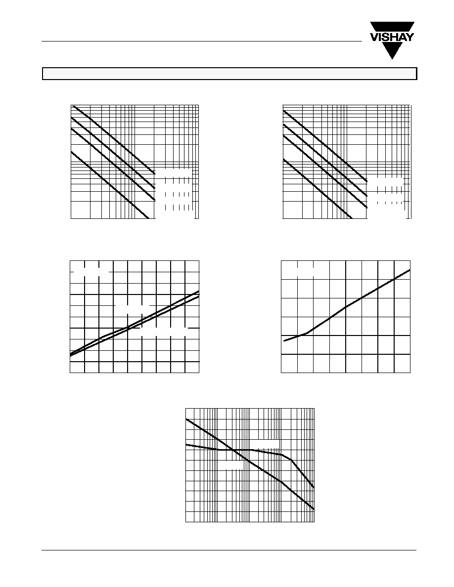
TYPICAL CHARACTERISTICS
1
--30
80
10
10000
Error Amplifier Gain and Phase vs. Frequency
Frequency (kHz)
Ga
i
n
(d
B
)
100
0
50
100
150
200
250
300
350
400
450
500
100 200 300 400 500 600 700 800 900 1000
R
t
= 100 k
Oscillator Dead Time vs. C
t
C
t
(pf)
SiP2800/01/02/04
Oscillator Frequency vs. R
t
and C
t
R
t
(k
)
O
s
c
illa
t
o
r
F
r
equenc
y
(
k
H
z
)
D
ead
T
i
me
(
n
S
)
0.7
0.8
0.9
1.0
1.1
1.2
1.3
--50
--25
0
25
50
75
100
125
150
CS = 0 V
COMP to CS Offset Voltage vs. Temperature
Temperature (
_
C)
SiP2803/05
Oscillator Frequency vs. R
t
and C
t
R
t
(k
)
O
s
c
illa
t
o
r
F
r
equenc
y
(
k
H
z
)
CO
M
P
to
CS
O
f
fs
e
t
(
V
)
70
60
50
40
30
20
10
0
--10
--20
1000
135
45
0
--45
90
P
has
e
(
_
)
C
t
= 100 pF
1000
100
10
10
100
1000
1000
100
10
10
100
1000
C
t
= 200 pF
C
t
= 330 pF
C
t
= 1000 pF
C
t
= 100 pF
C
t
= 200 pF
C
t
= 330 pF
C
t
= 1000 pF
SiP2803/05
SiP2800/01/02/04
Phase
Gain
SiP2800/01/02/03/04/05
Vishay Siliconix
New Product
Document Number: 72660
S-41623--Rev.C, 30-Aug-04
www.vishay.com
5
PIN CONFIGURATION
5
COMP
REF
FB
V
CC
CS
OUT
RC
GND
SOIC-8
6
7
8
2
3
4
1
Top View
COMP
FB
CS
RC
1
2
3
4
8
7
6
5
REF
V
CC
OUT
GND
TSSOP-8
Top View
D
ORDERING INFORMATION
SOIC-8
TSSOP-8
Part Number
Lead (Pb)-Free
Part Number
Marking Temperature
Part Number
Lead (Pb)-Free
Part Number
Marking Temperature
SiP2800DY-T1
SiP2800DY-T1--E3
2800
SiP2800DQ-T1
SiP2800DQ-T1--E3
2800
SiP2801DY-T1
SiP2801DY-T1--E3
2801
SiP2801DQ-T1
SiP2801DQ-T1--E3
2801
SiP2802DY-T1
SiP2802DY-T1--E3
2802
40 to 85
_
C
SiP2802DQ-T1
SiP2802DQ-T1--E3
2802
40 to 85
_
C
SiP2803DY-T1
SiP2803DY-T1--E3
2803
--40 to 85
_
C
SiP2803DQ-T1
SiP2803DQ-T1--E3
2803
--40 to 85
_
C
SiP2804DY-T1
SiP2804DY-T1--E3
2804
SiP2804DQ-T1
SiP2804DQ-T1--E3
2804
SiP2805DY-T1
SiP2805DY-T1--E3
2805
SiP2805DQ-T1
SiP2805DQ-T1--E3
2805
Additional voltage options are available.
PIN DESCRIPTION
Pin Number
Name
Function
1
COMP
Output of the Voltage Error Amplifier, and the inverting input to the PWM's Current Sense Comparator
2
FB
Inverting input of the Voltage Error Amplifier
3
CS
Non-inverting input of the PWM Current Sense Comparator, and inverting input of the Overcurrent Fault Comparator
(both comparators are fed from the output of the internal 100-ns Leading Edge Blanking circuit)
4
RC
Connection for the PWM Oscillator's timing resistor and timing capacitor
5
GND
Ground Pin.
6
OUT
PWM Output Signal (capable of driving
750 mA into the gate of an external MOSFET power switch)
7
V
CC
Positive supply voltage for the IC
8
REF
IC Reference Voltage

SiP2800/01/02/03/04/05
Vishay Siliconix
New Product
www.vishay.com
6
Document Number: 72660
S-41623--Rev.C, 30-Aug-04
DETAILED PIN DESCRIPTION
COMP
COMP is the output of the Voltage Error Amplifier (VEA). The
VEA is a low output impedance operational amplifier, providing
the input to the PWM cycle-by-cycle current limit comparator.
As the SiP280X series of parts use a true operational amplifier
for the VEA, the COMP terminal can both source and sink
current. To add flexibility to these parts, the VEA is internally
current limited, which allows OUT to be forced to zero duty
cycle by taking the COMP pin to GND.
The voltage on COMP is passed through an internal diode to
develop an offset voltage of approximately 0.6 V, and then
through a resistive divider with a gain of 0.606-V/V, before
being presented to the control input of the cycle-by-cycle
current limit comparator. Clamping the COMP pin to less than
the diode's forward voltage (i.e.,
<
0.5 V) will command the
current loop to deliver 0 A, by holding the control input of the
cycle-by-cycle current comparator at 0 V. Similarly, the current
loop will command the maximum inductor current on each
cycle when COMP is at 2.25 V or greater, which drives the
control input of the cycle-by-cycle current comparator to 1 V
(since [2.25 V -- 0.6 V]
�
0.606 V/V = 1 V).
The SiP280X series additionally features a built-in soft-start
function, which functions by clamping the output level of the
VEA to an internally generated voltage. This clamp will hold
COMP at a low voltage (V
COMP
0 V) until V
CC
and V
REF
are
at their proper levels. When these levels are appropriate for
circuit operation, the internal voltage will begin rising, at the
rate of 1 V/ms. This rising clamp level allows the voltage on the
COMP pin to rise, which in turn allows the voltage at the control
input of the cycle-by-cycle current comparator to increase. The
maximum soft-start interval occurs under conditions requiring
full duty cycle (50% or 100%, depending upon the part type),
and is given by the time required for the voltage on the
cycle-by-cycle current comparator's control input to reach 1 V.
Since 1 V at the control input to the comparator requires that
the COMP pin be at 2.25 V, the maximum soft-start interval is
approximately 2.25 ms.
CS
Input to both the cycle-by-cycle and overcurrent fault current
sense comparators. The cycle-by-cycle current limit
comparator is the mechanism by which the VEA's output
voltage commands the level of inductor or transformer current
during a given "on" interval, thereby regulating the overall
circuit's output. This comparator forms the inner loop of the two
loops used in current-mode regulation.
The overcurrent comparator has a trip threshold that is 50%
higher than that of the cycle-by-cycle comparator. Under
normal operating conditions, this comparator will not trip: its
purpose is to provide enhanced protection of the power path
components during severe faults (e.g., a short circuit). If the
overcurrent comparator is tripped by a fault condition, it will
command the SiP280X to do a "full-cycle restart." During this
restart, the power supply will be quickly driven to the "off" state,
and will be required to wait for five milliseconds (typical) before
restarting. When the supply does restart, it will do so using the
built-in soft-start function of the SiP280X.
The SiP280X family incorporates internal leading-edge
blanking on the CS pin, to keep any spurious voltages on the
CS pin from reaching the comparator inputs during the 100-ns
interval immediately following the rising edge on OUT (for
example, voltages due to capacitive charging currents).
Because of this internal leading-edge blanking, many
applications require no external RC filter on the CS input.
Compared to circuits requiring the use of an external RC filter
circuit, leading-edge blanking provides a shorter effective CS
to OUT propagation delay.
FB
FB is the inverting input of the VEA. Internally compared
against V
REF
/2 appearing on the VEA's non-inverting input. To
avoid stability problems, keep lead lengths to FB as short as
possible, and use good layout practices to minimize the stray
capacitances of components connected to this pin.
GND
The GND pin is both the reference ground and the power
ground for this part.
OUT
OUT is the output of a high-current driver capable of peak
currents in excess of
750 mA. OUT is therefore well suited
to driving the gates of power MOSFETs. This pin is specifically
held low when V
CC
is below the SiP280X's UVLO threshold, to
ensure a predictable system turn-on. Since the OUT pin is
internally connected to a low impedance CMOS buffer, it is
capable of rapid rail-to-rail transitions. This output topology
also mitigates the effects of undershoot and overshoot. For
this reason, external Schottky clamp diodes are generally not
required on this pin.
RC
RC is the oscillator frequency programming pin. F
OSC
is set by
the combination of R
T
and C
T
. The charging current for C
T
is
provided through R
T
, which is normally connected between
REF and the SiP280X RC pin. C
T
then connects from RC to
GND. Due to the high impedances encountered in low power
control circuits, this connection must be a short and quiet
return to GND (preferably by means of a dedicated signal
trace, separated from all other circuit functions).
The oscillator frequency for the SiP280X family of parts is
approximated by the following formulas:
For the SiP2800, SiP2801, SiP2802, and SiP2804:
D
F
OSC
(1.5)/R
T
C
T
For the SiP2803 and SiP2805:
D
F
OSC
(1.0)/R
T
C
T
Here R
T
is in ohms and C
T
is in farads.
More accurate formulas for F
OSC
are:
For the SiP2800, SiP2801, SiP2802 and SiP2804:
D
F
OSC
= 1/{[(C
T
+ C
STRAY
) x R
T
x 0.652] + [(C
T
+ C
STRAY
)
x R
DISCH
x 2.53] + T
DELAY
}

SiP2800/01/02/03/04/05
Vishay Siliconix
New Product
Document Number: 72660
S-41623--Rev.C, 30-Aug-04
www.vishay.com
7
For the SiP2803 and SiP2805:
D
F
OSC
= 1/{[(C
T
+ C
STRAY
) x R
T
x 0.93] + [(C
T
+ C
STRAY
) x
R
DISCH
x 2.53] + T
DELAY
}
Here R
T
is in ohms and C
T
is in farads, R
DISCH
is the value of
the resistor through which C
T
is discharged (normally an
on-chip 130-
resistor, unless the circuit is configured with
additional external discharge-path resistance), and t
DELAY
is
an inherent internal comparator delay time of 100 ns. The
capacitance associated with the RC pin is approximately
7.5 pF, and should be included as a part of C
STRAY
.
Note that the SiP2801, SiP2804, and SiP2805 have an internal
toggle flip-flop at the output of the oscillator, to ensure that the
output duty cycle never exceeds 50%. This divides the
frequency appearing at the OUT pin to one-half of the oscillator
frequency for these three parts.
Values of R
T
below 10 k are not recommended. Low values of
R
T
cause high circuit operating currents, and very low values
will prevent the oscillator from properly discharging C
T
.
REF
The reference generator block of the Si280X provides an
accurate and stable 4.0 V or 5.0 V (depending upon part
number), which is available at this pin of the IC. This voltage
is also used internally for other functions on the IC. One of
these uses is as the logic power supply for high speed
switching logic on the IC; this, and stability concerns, make it
important to bypass V
REF
to GND with a good quality 0.1-
m
F
ceramic capacitor, as close to the part as possible. An
electrolytic or tantalum capacitor may be used in addition to the
ceramic capacitor. When 1 V < V
CC
< the UVLO threshold,
REF is pulled to ground through a 5-k
resistor. Hence, REF
can also be used as an output to indicate the part's V
CC
status.
V
CC
V
CC
is the positive power connection for the SiP280X
controller IC, and should be the most positive terminal on the
part. In normal operation, V
CC
is powered through a current
limiting resistor. The required start-up supply current will
generally be on the order of 100
m
A with V
CC
below the UVLO
voltage of the SiP280X, and can remain at or below 500-
m
A
total supply current once the part starts switching. To prevent
the IC from being damaged by overvoltage conditions, each of
the SiP2800 family of parts has an internal clamp (effectively
a 12.5-V Zener diode) between V
CC
and GND. If the part's V
CC
pin is current-fed through an appropriate dropping resistor, the
V
CC
pin will never exceed its rated voltage, nor will the the
device as a whole exceed its rated power dissipation. This
does require knowing what the operating current of the IC will
be, so that the value of the dropping resistor can be calculated.
A good estimate of the actual operating current (I
CC
) may be
made by summing three components:
(a) Any external current loading on the V
CC
or REF pins
(b) The operating current required by the IC itself, and
(c) The drive current (I
DRIVE
) required by the external
power switch.
Item (a) in the above list is a static dc value, and can generally
be calculated with good accuracy. Item (b) will increase with
operating frequency, but will be fixed for a given value of F
OSC
.
Item (c) is usually the dominant term in the calculation of I
CC
,
as the power required to drive the external power switch will
typically increase as F
OUT
is increased. The most common
example of this is seen in driving the gate of a power MOSFET.
In such applications, the gate capacitances must be charged
once each switching cycle. This calculation is simplified by
using the gate charge term given by most MOSFET
manufacturers, allowing the use of the formula:
I
DRIVE
= F
OUT
�
Q
g
of the chosen MOSFET.
A first approximation of the necessary dropping resistor value
is then given by:
R = [(Nominal V
SUPPLY
) � 12 V]/(Nominal I
CC
)
Here R is in ohms and I
CC
is in amperes.
The resistor limiting the current into the V
CC
pin should be
selected such that I
CC(min)
equals the worst-case maximum
sum of the above currents, while holding I
CC(max)
to as low a
value above that number as practicable (for best overall
efficiency), and never more than 25 mA above that number (to
avoid exceeding the IC's internal clamp diode ratings). V
CC
must be bypassed to GND with a good quality 0.1-
m
F ceramic
capacitor, as close to the part as possible. This will help avoid
problems created by high-frequency noise on the power
supply of the part. An electrolytic or tantalum capacitor may be
placed in parallel with the ceramic capacitor if more
capacitance is needed or desired.
SiP2800/01/02/03/04/05
Vishay Siliconix
New Product
www.vishay.com
8
Document Number: 72660
S-41623--Rev.C, 30-Aug-04
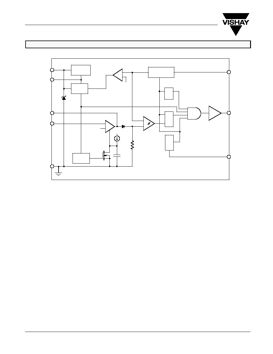
FUNCTIONAL BLOCK DIAGRAM
CS
OUT
RC
COMP
V
CC
FB
GND
T Q
S Q
R
OSC
Leading Edge
Blanking
Reference
Voltage
UVLO
Soft-Start
REF
SiP2801/4/5 Only
1.5 V
REF/2
Overcurrent
Comparator
--
+
+
--
Voltage Error
Amplifier
PWM
Comparator
13.5 V
--
+