Pb-free
Available
SiP42101
Vishay Siliconix
New Product
Document Number: 73176
S-50265--Rev. B, 21-Feb-05
www.vishay.com
1
Half-Bridge N-Channel MOSFET Driver for Motor Control
FEATURES
APPLICATIONS
D 5-V Gate Drive
D Undervoltage Lockout
D Internal Bootstrap Diode
D Adaptive Shoot-Through Protection
D Motor Braking
D Shutdown Control
D Matched Rising and Falling Propagation Delays
D Drive MOSFETs In 4.5- to 50-V Systems
D H-Bridge Motor Controls
D 3-Phase Motor Controls
DESCRIPTION
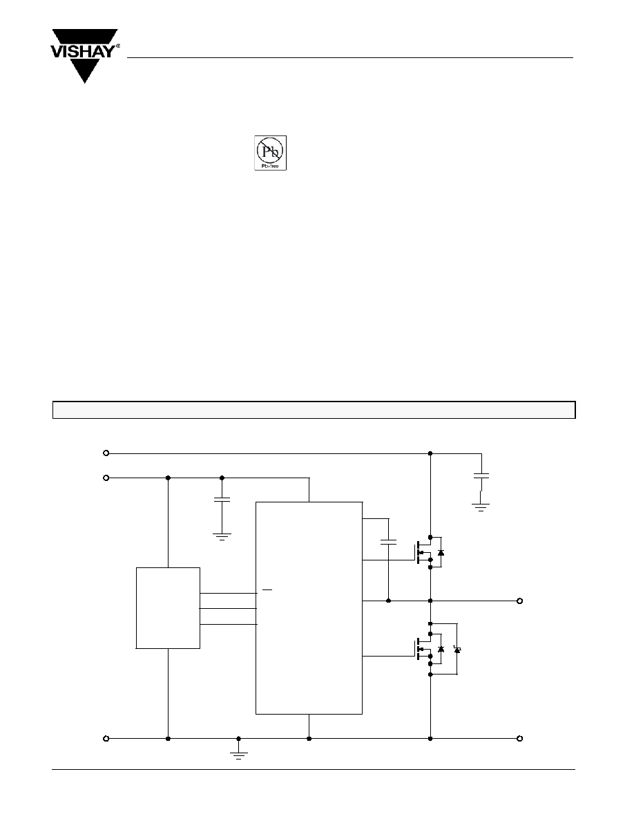
The SiP42101 is a high-speed half-bridge MOSFET driver with
adaptive shoot-through protection for motor driving
applications. The high-side driver is bootstrapped to allow
driving n-channel MOSFETs. The Brake pin forces the lowside
MOSFET on, providing a braking function in H-bridge and
3-phase topologies.
The SiP42101 comes with adaptive shoot-through protection
to prevent simultaneous conduction of the external MOSFETs.
The SiP42101 is available in both standard and lead (Pb)-free
10-Pin MLP33 packages and is specified to operate over the
industrial temperature range of -40 _C to 85 _C.
FUNCTIONAL BLOCK DIAGRAM
Controller
PWM
GND
V
DD
Motor
Winding
GND
GND
+5 V
+5 to 50 V
BOOT
OUT
H
LX
OUT
L
SiP42101
BRAKE
SD
SiP42101
Vishay Siliconix
New Product
www.vishay.com
2
Document Number: 73176
S-50265--Rev. B, 21-Feb-05
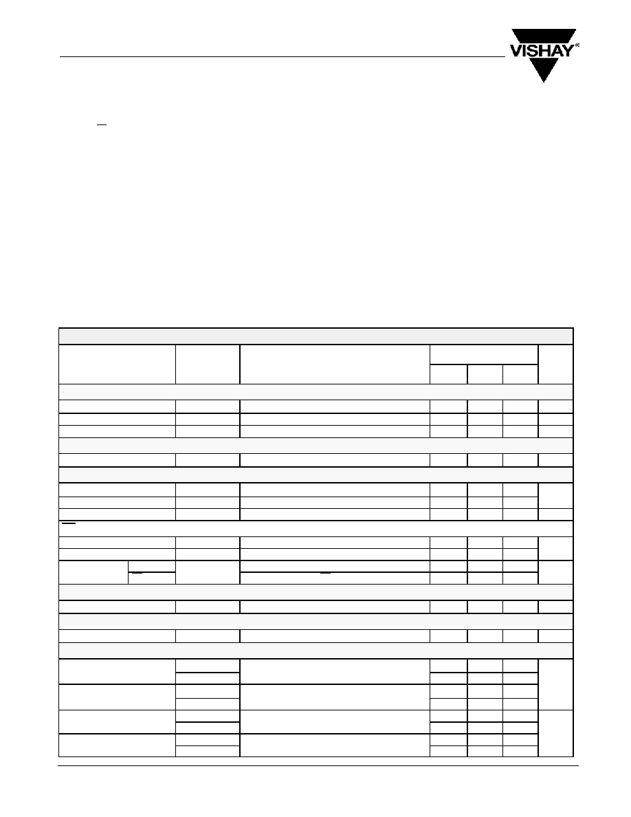
ABSOLUTE MAXIMUM RATINGS (ALL VOLTAGES REFERENCED TO GND = 0 V)
V
DD
, PWM, SD, BRAKE
7 V
. . . . . . . . . . . . . . . . . . . . . . . . . . . . . . . . . . . . . . . . .
LX, BOOT
55 V
. . . . . . . . . . . . . . . . . . . . . . . . . . . . . . . . . . . . . . . . . . . . . . . . . . .
BOOT to LX
7 V
. . . . . . . . . . . . . . . . . . . . . . . . . . . . . . . . . . . . . . . . . . . . . . . . . .
Storage Temperature
-40 to 150_C
. . . . . . . . . . . . . . . . . . . . . . . . . . . . . . . . . .
Operating Junction Temperature
125_C
. . . . . . . . . . . . . . . . . . . . . . . . . . . . . .
Power Dissipation
a,b
MLP-33
960 mW
. . . . . . . . . . . . . . . . . . . . . . . . . . . . . . . . . . . . . . . . . . . . . . . . .
Thermal Impedance (Q
JA
)
a,b
MLP-33
105_C/W
. . . . . . . . . . . . . . . . . . . . . . . . . . . . . . . . . . . . . . . . . . . . . . . . .
Notes
a.
Device mounted with all leads soldered or welded to PC board.
a.
Derate 9.6 mW/_C
Stresses beyond those listed under "Absolute Maximum Ratings" may cause permanent damage to the device. These are stress ratings only, and functional operation
of the device at these or any other conditions beyond those indicated in the operational sections of the specifications is not implied. Exposure to absolute maximum rating
conditions for extended periods may affect device reliability.
RECOMMENDED OPERATING RANGE (ALL VOLTAGES REFERENCED TO GND = 0 V)
V
DD
4.5 V to 5.5 V
. . . . . . . . . . . . . . . . . . . . . . . . . . . . . . . . . . . . . . . . . . . . . . . . .
V
BOOT
4.5 V to 50 V
. . . . . . . . . . . . . . . . . . . . . . . . . . . . . . . . . . . . . . . . . . . . . .
C
BOOT
100 nF to 1 mF
. . . . . . . . . . . . . . . . . . . . . . . . . . . . . . . . . . . . . . . . . . . . .
Operating Temperature Range
-40 to 85_C
. . . . . . . . . . . . . . . . . . . . . . . . . . .
SPECIFICATIONS
a
Test Conditions Unless Specified
Limits
Parameter
Symbol
V
DD
= 5 V, V
BOOT
- V
LX
= 5 V, C
LOAD
= 3 nF
T
A
= -40 to 85_C
Min
a
Typ
b
Max
a
Unit
Power Supplies
Supply Voltage
V
DD
4.5
5.5
V
Quiescent Current
I
DDQ
f
PWM
= 1 MHz, C
LOAD
= 0
2.2
3.0
mA
Shutdown Current
I
SD
1
mA
Reference Voltage
Break-Before-Make
V
BBM
1
V
PWM Input
Input High
V
IH
4.0
V
DD
V
Input Low
V
IL
0.5
V
Bias Current
I
B
"0.3
"1
mA
SD, BRAKE Inputs
Input High
V
IH
2.0
V
DD
V
Input Low
V
IL
1.0
V
Bias Current
Brake
I
B
"1
mA
Bias Current
SD
I
B
SD = 5 V
3.5
7
mA
High-Side Undervoltage Lockout
Threshold
V
UVHS
Rising or Falling
2.5
3.35
3.75
V
Bootstrap Diode
Forward Voltage
V
F
I
F
= 10 mA, T
A
= 25_C
0.70
0.76
0.82
V
MOSFET Drivers
High-Side Drive Current
c
I
PKH(source)
0.9
High-Side Drive Current
c
I
PKH(sink)
1.1
A
Low-Side Drive Current
c
I
PKL(source)
0.8
A
Low-Side Drive Current
c
I
PKL(sink)
1.5
High Side Driver Impedance
R
DH(source)
2.5
3.8
High-Side Driver Impedance
R
DH(sink)
2.2
3.3
W
Low Side Driver Impedance
R
DL(source)
3.4
5.1
W
Low-Side Driver Impedance
R
DL(sink)
1.4
2.1
SiP42101
Vishay Siliconix
New Product
Document Number: 73176
S-50265--Rev. B, 21-Feb-05
www.vishay.com
3
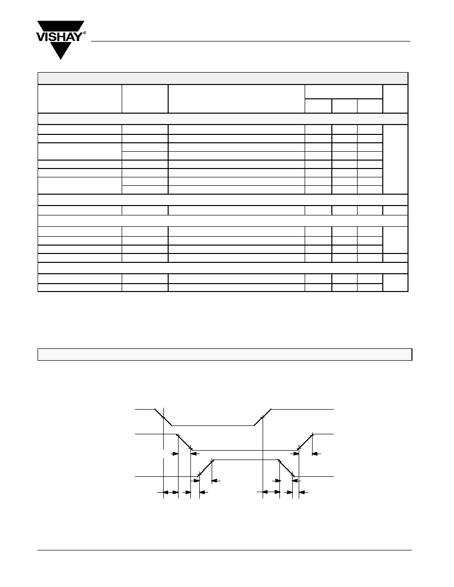
SPECIFICATIONS
a
Limits
Test Conditions Unless Specified
V
DD
= 5 V, V
BOOT
- V
LX
= 5 V, C
LOAD
= 3 nF
T
A
= -40 to 85_C
Parameter
Unit
Max
a
Typ
b
Min
a
Test Conditions Unless Specified
V
DD
= 5 V, V
BOOT
- V
LX
= 5 V, C
LOAD
= 3 nF
T
A
= -40 to 85_C
Symbol
MOSFET Drivers
High-Side Rise Time
t
rH
10% - 90%
32
40
High-Side Fall Time
t
fH
90% - 10%
36
45
High Side Propagation Delay
c
t
d(off)H
See Timing Waveforms
20
High-Side Propagation Delay
c
t
d(on)H
See Timing Waveforms
30
ns
Low-Side Rise Time
t
rL
10% - 90%
45
55
ns
Low-Side Fall Time
t
fL
90% - 10%
20
30
Low Side Propagation Delay
c
t
d(off)L
See Timing Waveforms
30
Low-Side Propagation Delay
c
t
d(on)L
See Timing Waveforms
30
LX Timer
LX Falling Timeout
c
t
LX
420
ns
V
DD
Undervoltage Lockout
Threshold Rising
V
UVLOR
4.35
4.5
Threshold Falling
V
UVLOF
3.7
4.1
V
Hysteresis
V
H
0.4
Power on Reset Time
c
2.5
ms
Thermal Shutdown
Temperature
T
SD
Temperature Rising
165
_C
Hysteresis
T
H
Temperature Falling
25
_C
Notes
a.
The algebraic convention whereby the most negative value is a minimum and the most positive a maximum (-40_ to 85_C).
b.
Typical values are for DESIGN AID ONLY, not guaranteed nor subject to production testing and are measured at V
DD
= 5V unless otherwise noted.
c.
Guaranteed by design.
TIMING WAVEFORMS
t
d(off)H
t
d(off)L
PWM
OUT
H
OUT
L
t
d(on)L
t
d(on)H
10%
90%
50%
90%
10%
10%
10%
50%
90%
90%
t
fL
t
rH
t
rL
t
fH
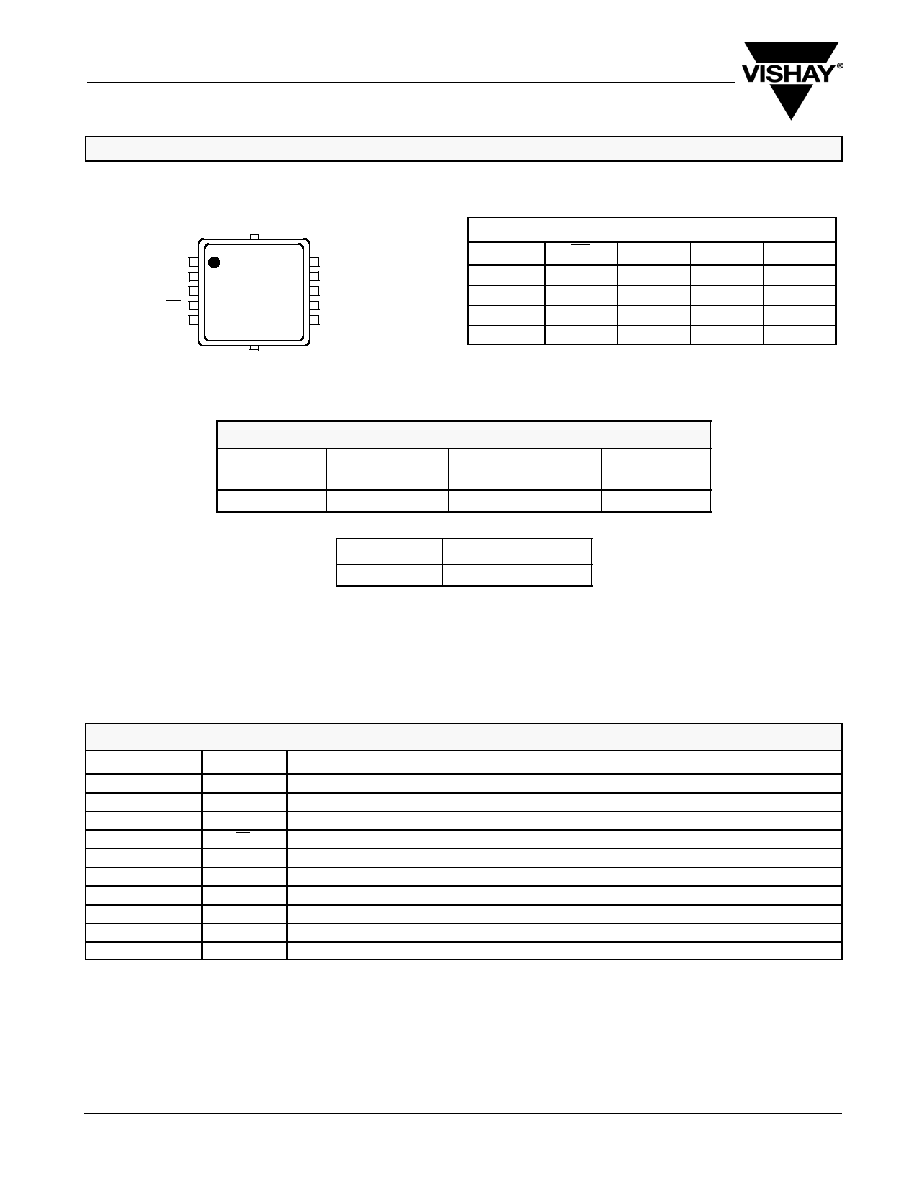
2
3
4
10
9
8
7
OUT
H
BOOT
PWM
SD
LX
BRAKE
NC
V
DD
Top View
5
GND
6
OUT
L
MLP33
SiP42101
Vishay Siliconix
New Product
www.vishay.com
4
Document Number: 73176
S-50265--Rev. B, 21-Feb-05
PIN CONFIGURATION AND TRUTH TABLE
TRUTH TABLE
PWM
SD
BRAKE
OUT
H
OUT
L
L
H
L
L
H
H
H
L
H
L
X
H
H
L
H
X
L
X
L
L
ORDERING INFORMATION
Standard
Part Number
Lead(Pb)-Free
Part Number
Temperature Range
Marking
SiP42101DM-T1
SiP42101DM-T1--E3
-40 to 85_C
42101
Eval Kit
Temperature Range
SiP42101DB
-40 to 85_C
PIN DESCRIPTION
Pin Number
Name
Function
1
OUT
H
High-side MOSFET gate drive
2
BOOT
Bootstrap supply for high-side driver. A capacitor connects between BOOT and LX.
3
PWM
Input signal for the MOSFET drivers
4
SD
Shuts down the driver
5
GND
Ground
6
OUT
L
Synchronous or low-side MOSFET gate drive
7
V
DD
+5-V supply
8
NC
No Connect
9
BRAKE
Forces OUT
L
high and OUT
H
low
10
LX
Connection to source of high-side MOSFET, drain of the low-side MOSFET, and the inductor
SiP42101
Vishay Siliconix
New Product
Document Number: 73176
S-50265--Rev. B, 21-Feb-05
www.vishay.com
5
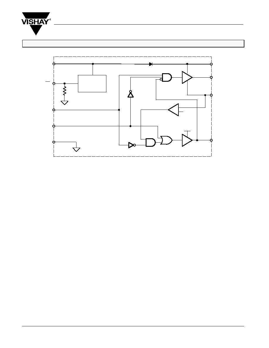
FUNCTIONAL BLOCK DIAGRAM
Figure 1.
PWM
GND
V
DD
OUT
H
LX
OUT
L
OTP
V
DD
BOOT
V
BBM
-
+
UVLO
SD
BRAKE
DETAILED OPERATION
PWM
The PWM pin controls the switching of the external MOSFETs.
The driver logic operates in a noninverting configuration. The
PWM input stage should be driven by a signal with fast
transition times, like those provided by a PWM controller or
logic gate, (<200 ns). The PWM input functions as a logic input
and is not intended for applications where a slow changing
input voltage is used to generate a switching output when the
input switching threshold voltage is reached.
Low-Side Driver
The supplies for the low-side driver are V
DD
and GND. During
shutdown, OUT
L
is held low.
High-Side Driver
The high-side driver is isolated from the substrate to create a
floating high-side driver so that an n-channel MOSFET can be
used for the high-side switch. The supplies for the high-side
driver are BOOT and LX. The voltage is supplied by a floating
bootstrap capacitor, which is continually recharged by the
switching action of the output. During shutdown OUT
H
is held
low.
Bootstrap Circuit
The internal bootstrap diode and a bootstrap capacitor form a
charge pump that supplies voltage to the BOOT pin. An
integrated bootstrap diode replaces the external Schottky
diode needed for the bootstrap circuit; only a capacitor is
necessary to complete the bootstrap circuit. The bootstrap
capacitor is sized according to,
C
BOOT
= (Q
GATE
/DV
BOOT - LX
) x 10
where Q
GATE
is the gate charge needed to turn on the
high-side MOSFET and DV
BOOT
- LX
is the amount of droop
allowed in the bootstrapped supply voltage when the high-side
MOSFET is driven high. The bootstrap capacitor value is
typically 0.1 mF to 1 mF. The bootstrap capacitor voltage rating
must be greater than V
DD
+ 5 V to withstand transient spikes
and ringing.
Shoot-Through Protection
The external MOSFETs are prevented from conducting at the
same time during transitions. Break-before-make circuits
monitor the voltages on the LX pin and the OUT
L
pin and
control the switching as follows: When the signal on PWM goes
low, OUT
H
will go low after an internal propagation delay. After
the voltage on LX falls below 1 V by the inductor action, the
low-side driver is enabled and OUT
L
goes high after some
delay. When the signal on PWM goes high, OUT
L
will go low
after an internal propagation delay. After the voltage on OUT
L
drops below 1 V the high-side driver is enabled and OUT
H
will
go high after an internal propagation delay. If LX does not drop
below 1 V within 400 ns after OUT
H
goes low, OUT
L
is forced
high until the next PWM transition.