Vishay General Semiconductor
SS12 thru SS16
Document Number 88746
06-Jul-06
www.vishay.com
1
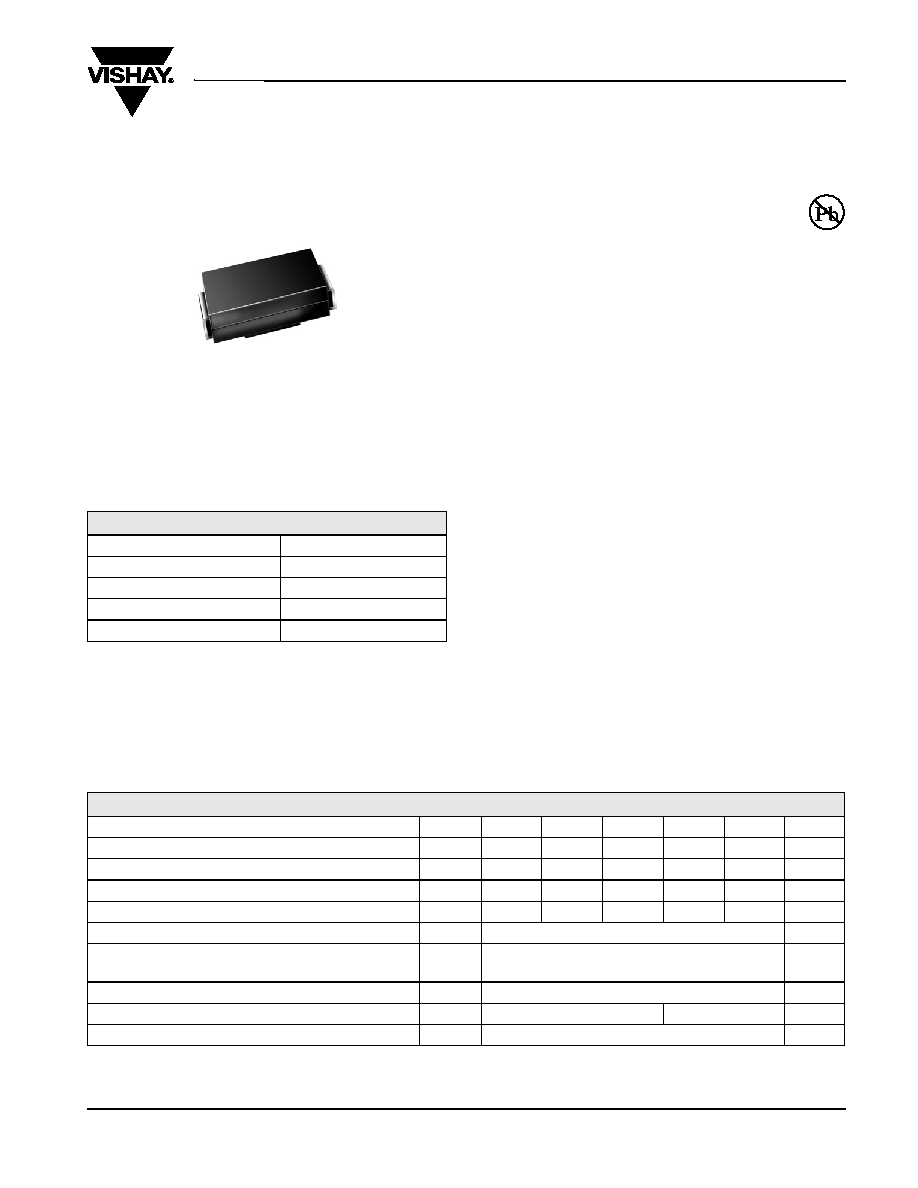
Surface Mount Schottky Barrier Rectifier
FEATURES
∑ Low profile package
∑ Ideal for automated placement
∑ Guardring for overvoltage protection
∑ Low power losses, high efficiency
∑ Low forward voltage drop
∑ High surge capability
∑ Meets MSL level 1, per J-STD-020C, LF max peak
of 260 ∞C
∑ Solder Dip 260 ∞C, 40 seconds
∑ Component in accordance to RoHS 2002/95/EC
and WEEE 2002/96/EC
TYPICAL APPLICATIONS
For use in low voltage, high frequency inverters, free-
wheeling, dc-to-dc converters, and polarity protection
applications.
MECHANICAL DATA
Case: DO-214AC (SMA)
Epoxy meets UL 94V-0 flammability rating
Terminals: Matte tin plated leads, solderable per
J-STD-002B and JESD22-B102D
E3 suffix for commercial grade, HE3 suffix for high
reliability grade (AEC Q101 qualified)
Polarity: Color band denotes the cathode end
DO-214AC (SMA)
MAJOR RATINGS AND CHARACTERISTICS
I
F(AV)
1.0 A
V
RRM
20 V to 60 V
I
FSM
40 A
V
F
0.50 V, 0.75 V
T
j
max.
125 ∞C, 150 ∞C
MAXIMUM RATINGS (T
A
= 25 ∞C unless otherwise noted)
PARAMETER
SYMBOL
SS12 SS13 SS14 SS15 SS16 UNIT
Device
marking
code
S2 S3 S4 S5 S6 V
Maximum repetitive peak reverse voltage
V
RRM
20
30
40
50
60
V
Maximum RMS voltage
V
RMS
14
21
28
35
42
V
Maximum DC blocking voltage
V
DC
20
30
40
50
60
V
Maximum average forward rectified current at T
L
(see Fig. 1)
I
F(AV)
1.0
A
Peak forward surge current 8.3 ms single half sine-wave
superimposed on rated load
I
FSM
40 A
Voltage rate of change (rated V
R
) dv/dt 10000 V/µs
Operating junction temperature range
T
J
- 65 to + 125
- 65 to + 150
∞C
Storage temperature range
T
STG
- 65 to + 150
∞C
www.vishay.com
2
Document Number 88746
06-Jul-06
Vishay General Semiconductor
SS12 thru SS16
Note:
(1) Pulse test: 300 µs pulse width, 1 % duty cycle
Note:
(1) P.C.B. mounted with 0.2 x 0.2" (5.0 x 5.0 mm) copper pad areas
RATINGS AND CHARACTERISTICS CURVES
(T
A
= 25
∞C unless otherwise noted)
ELECTRICAL CHARACTERISTICS (T
A
= 25 ∞C unless otherwise noted)
PARAMETER
TEST
CONDITIONS SYMBOL
SS12 SS13 SS14 SS15 SS16 UNIT
Maximum instantaneous forward
voltage
(1)
at 1.0 A
V
F
0.50
0.75
V
Maximum DC reverse current at rated
DC blocking voltage
(1)
T
A
= 25 ∞C
I
R
0.2
mA
T
A
= 100 ∞C
6.0
5.0
THERMAL CHARACTERISTICS
(T
A
= 25 ∞C unless otherwise noted)
PARAMETER
SYMBOL
SS12 SS13 SS14 SS15 SS16 UNIT
Typical thermal resistance
(1)
R
JA
R
JL
88
28
∞C/W
ORDERING INFORMATION
PREFERRED P/N
UNIT WEIGHT (g)
PREFERRED PACKAGE CODE
BASE QUANTITY
DELIVERY MODE
SS14-E3/61T
0.064
61T
1800
7" Diameter Plastic Tape & Reel
SS14-E3/5AT
0.064
5AT
7500
13" Diameter Plastic Tape & Reel
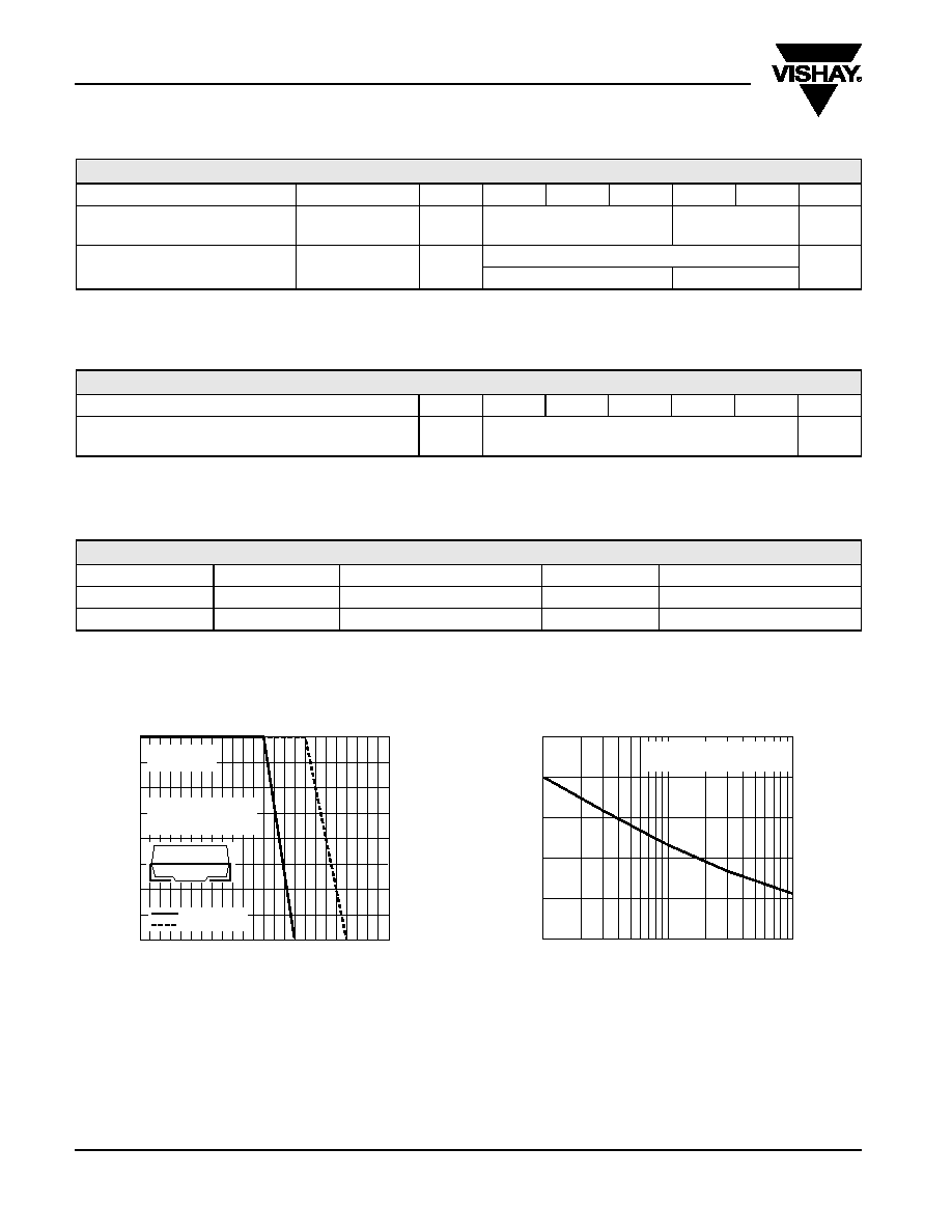
Figure 1. Forward Current Derating Curve
50
70
90
110
130
150
0
0.5
1.0
170
Resistive or
Inductive Load
P. C. B. Mounted on
0.2 x 0.2" (5.0 x 5.0 mm)
Copper Pad Areas
SS12 - SS14
SS15 & SS16
Lead Temperature (∞C)
A
v
er
age F
o
r
w
ard C
u
rrent (A)
Figure 2. Maximum Non-Repetitive Peak Forward Surge Current
1
10
100
0
10
20
30
40
50
At rated T
L
8.3 ms Single Half Sine-Wave
Number of Cycles at 60 Hz
Pe
a
k
F
o
r
w
ard S
u
rge C
u
rrent (A)
Document Number 88746
06-Jul-06
www.vishay.com
3
SS12 thru SS16
Vishay General Semiconductor
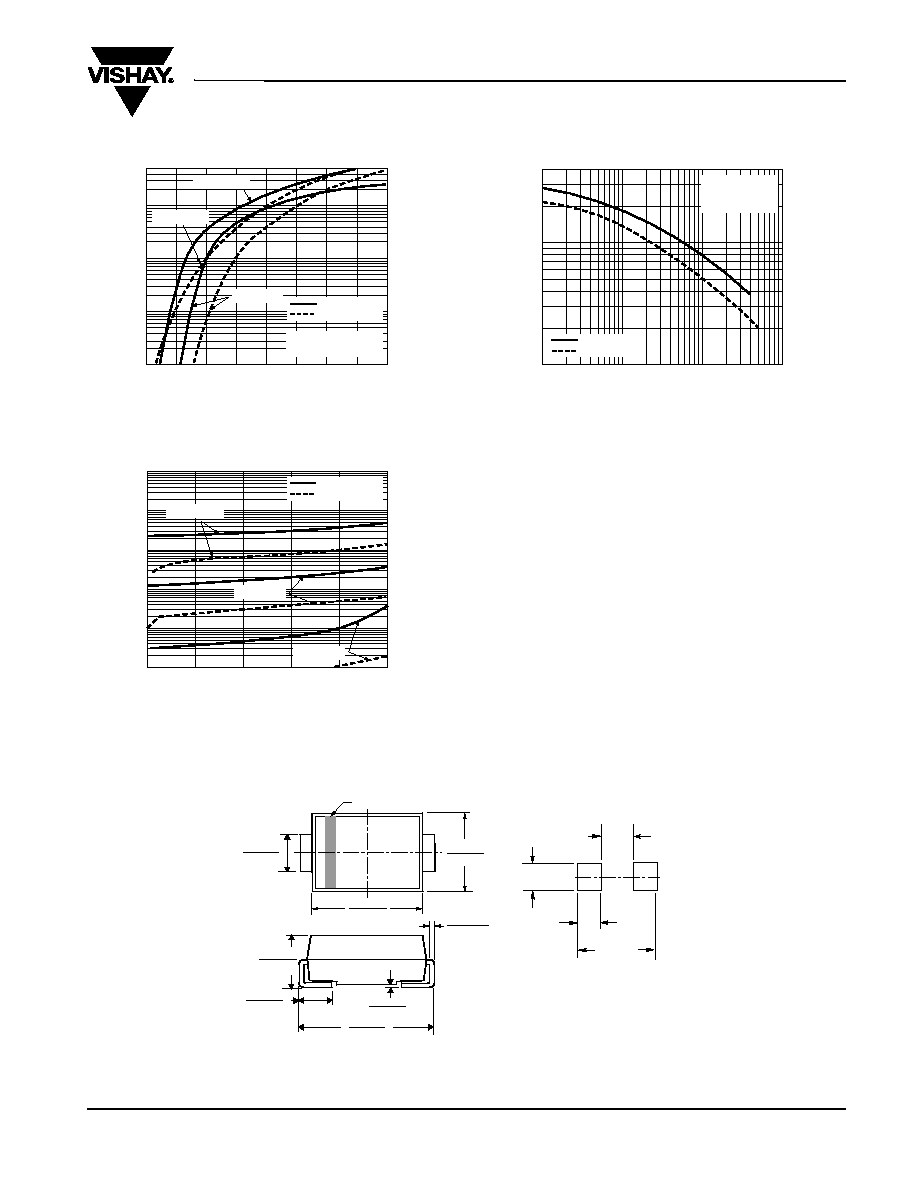
PACKAGE OUTLINE DIMENSIONS in inches (millimeters)
Figure 3. Typical Instantaneous Forward Characteristics
Figure 4. Typical Reverse Characteristics
0.2
0.4
0.6
0.8
1.0
1.2
1.4
1.6
1
10
50
0
0.01
0.1
Instantaneous Forward Voltage (V)
Instantaneo
u
s F
o
r
w
ard C
u
rrent (A)
SS12 - SS14
SS15 & SS16
Pulse Width = 300 µs
1 % Duty Cycle
T
j
= 150 ∞C
T
j
= 125 ∞C
T
j
= 25 ∞C
0
20
40
60
0.001
0.01
0.1
1
10
100
80
100
Percent of Rated Peak Reverse Voltage (%)
Instantaneo
u
s Re
v
erse C
u
rrent (mA)
T
j
= 75 ∞C
T
j
= 125 ∞C
T
j
= 25 ∞C
SS12 - SS14
SS15 & SS16
Figure 5. Typical Junction Capacitance
100
10
10
100
400
0.1
1
Reverse Voltage (V)
J
u
nction Capaci
tance (pF)
T
j
= 25 ∞C
f = 1.0 MHz
V
sig
= 50 mVp-p
SS12 - SS14
SS15 & SS16
0.157 (3.99)
0.177 (4.50)
0.006 (0.152)
0.012 (0.305)
0.030 (0.76)
0.060 (1.52)
0.008 (0.203)
0.194 (4.93)
0.208 (5.28)
0.100 (2.54)
0.110 (2.79)
0.078 (1.98)
0.090 (2.29)
0.049 (1.25)
0.065 (1.65)
Cathode Band
0 (0)
DO-214AC (SMA)
0.074 MAX.
(1.88 MAX.)
0.208
(5.28) REF
0.066 MIN.
(1.68 MIN.)
0.060 MIN.
(1.52 MIN.)
Mounting Pad Layout

Legal Disclaimer Notice
Vishay
Document Number: 91000
www.vishay.com
Revision: 08-Apr-05
1
Notice
Specifications of the products displayed herein are subject to change without notice. Vishay Intertechnology, Inc.,
or anyone on its behalf, assumes no responsibility or liability for any errors or inaccuracies.
Information contained herein is intended to provide a product description only. No license, express or implied, by
estoppel or otherwise, to any intellectual property rights is granted by this document. Except as provided in Vishay's
terms and conditions of sale for such products, Vishay assumes no liability whatsoever, and disclaims any express
or implied warranty, relating to sale and/or use of Vishay products including liability or warranties relating to fitness
for a particular purpose, merchantability, or infringement of any patent, copyright, or other intellectual property right.
The products shown herein are not designed for use in medical, life-saving, or life-sustaining applications.
Customers using or selling these products for use in such applications do so at their own risk and agree to fully
indemnify Vishay for any damages resulting from such improper use or sale.