FEATURES
D
TrenchFET
r
Power MOSFET
D
175
_
C Junction Temperature
APPLICATIONS
D
Automtoive 12-V Boardnet
SUD50P06-15L
Vishay Siliconix
New Product
Document Number: 72250
S-31673--Rev. B 11-Aug-03
www.vishay.com
1
P-Channel 60-V (D-S), 175
_
C MOSFET
PRODUCT SUMMARY
V
DS
(V)
r
DS(on)
(
W
)
I
D
(A)
-60
0.015 @ V
GS
= -10 V
-50
d
-60
0.020 @ V
GS
= -4.5 V
-50
S
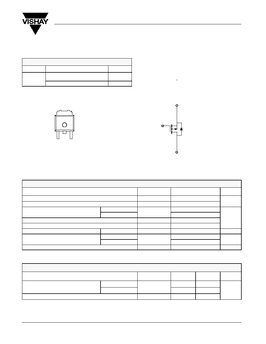
G
D
P-Channel MOSFET
TO-252
S
G
D
Top View
Drain Connected to Tab
Ordering Information: SUD50P06-15L
ABSOLUTE MAXIMUM RATINGS (T
A
= 25_C UNLESS OTHERWISE NOTED)
Parameter
Symbol
Limit
Unit
Drain-Source Voltage
V
DS
-60
V
Gate-Source Voltage
V
GS
"
20
V
Continuous Drain Current
T
C
= 25
_
C
I
D
-50
d
Continuous Drain Current
(T
J
= 175
_
C)
T
C
= 125
_
C
I
D
-39
A
Pulsed Drain Current
I
DM
-80
A
Avalanche Current
I
AR
-50
Repetitive Avalanche Energy
a
L = 0.1 mH
E
AR
125
mJ
Power Dissipation
T
C
= 25
_
C
P
D
136
c
W
Power Dissipation
T
A
= 25
_
C
P
D
3
b, c
W
Operating Junction and Storage Temperature Range
T
J
, T
stg
-55 to 175
_
C
THERMAL RESISTANCE RATINGS
Parameter
Symbol
Typical
Maximum
Unit
J
ti
t A bi t
b
t
v
10 sec
R
15
18
Junction-to-Ambient
b
Steady State
R
thJA
40
50
_
C/W
Junction-to-Case
R
thJC
0.82
1.1
C/W
Notes:
a.
Duty cycle
v
1%.
b.
When mounted on 1" square PCB (FR-4 material).
c.
See SOA curve for voltage derating.
d.
Package limited.
SUD50P06-15L
Vishay Siliconix
New Product
www.vishay.com
2
Document Number: 72250
S-31673--Rev. B 11-Aug-03
SPECIFICATIONS (T
J
= 25_C UNLESS OTHERWISE NOTED)
Parameter
Symbol
Test Condition
Min
Typ
Max
Unit
Static
Drain-Source Breakdown Voltage
V
(BR)DSS
V
GS
= 0 V, I
D
= -250
m
A
-
60
V
Gate Threshold Voltage
V
GS(th)
V
DS
= V
GS
, I
D
= -250
m
A
-1
-3
V
Gate-Body Leakage
I
GSS
V
DS
= 0 V, V
GS
=
"
20 V
"
100
nA
V
DS
= -48 V, V
GS
= 0 V
-1
Zero Gate Voltage Drain Current
I
DSS
V
DS
= -48 V, V
GS
= 0 V, T
J
= 125
_
C
-50
mA
g
DSS
V
DS
= -48 V, V
GS
= 0 V, T
J
= 175
_
C
-150
m
On-State Drain Current
a
I
D(on)
V
DS
= -5 V, V
GS
= -10 V
-50
A
V
GS
= -10 V, I
D
= -17 A
0.012
0.015
Drain Source On State Resistance
a
r
DS( )
V
GS
= -10 V, I
D
= -50 A, T
J
= 125
_
C
0.025
W
Drain-Source On-State Resistance
a
r
DS(on)
V
GS
= -10 V, I
D
= -50 A, T
J
= 175
_
C
0.030
W
V
GS
= -4.5 V, I
D
= -14 A
0.020
Forward Transconductance
a
g
fs
V
DS
= -15 V, I
D
= -17 A
61
S
Dynamic
b
Input Capacitance
C
iss
4950
Output Capacitance
C
oss
V
GS
= 0 V, V
DS
= -25 V, f = 1 MHz
480
pF
Reversen Transfer Capacitance
C
rss
405
Total Gate Charge
c
Q
g
110
165
Gate-Source Charge
c
Q
gs
V
DS
= -30 V,
V
GS
= -10 V, I
D
= -50 A
19
nC
Gate-Drain Charge
c
Q
gd
DS
,
GS
,
D
28
Turn-On Delay Time
c
t
d(on)
15
23
Rise Time
c
t
r
V
DD
= -30 V, R
L
= 0.6
W
70
105
ns
Turn-Off Delay Time
c
t
d(off)
V
DD
= 30 V, R
L
= 0.6
W
I
D
]
-50 A, V
GEN
= -10 V, R
G
= 6
W
175
260
ns
Fall Time
c
t
f
D
GEN
G
175
260
Source-Drain Diode Ratings and Characteristics (T
C
= 25
_
C)
b
Continuous Current
I
s
-50
A
Pulsed Current
I
SM
-80
A
Forward Voltage
a
V
SD
I
F
= -50 A, V
GS
= 0 V
1.0
1.6
V
Reverse Recovery Time
t
rr
I
F
= -50 A, di/dt = 100 A/
m
s
45
70
ns
Notes:
a.
Pulse test; pulse width
v
300
m
s, duty cycle
v
2%.
b.
Guaranteed by design, not subject to production testing.
c.
Independent of operating temperature.
SUD50P06-15L
Vishay Siliconix
New Product
Document Number: 72250
S-31673--Rev. B 11-Aug-03
www.vishay.com
3
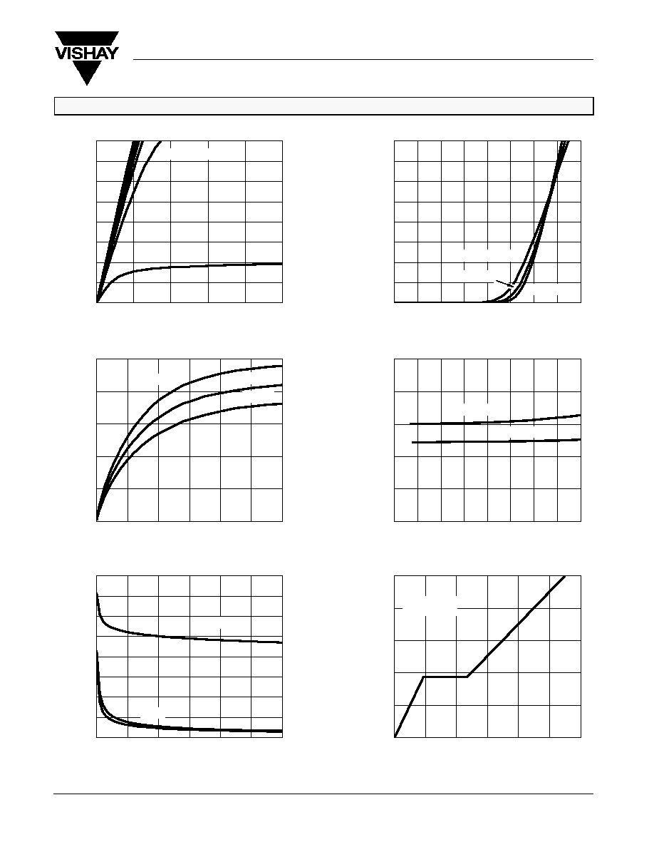
TYPICAL CHARACTERISTICS (25_C UNLESS NOTED)
0
2
4
6
8
10
0
20
40
60
80
100
120
0.000
0.005
0.010
0.015
0.020
0.025
0
10
20
30
40
50
60
70
80
0
1000
2000
3000
4000
5000
6000
7000
8000
0
10
20
30
40
50
60
0
20
40
60
80
100
0
10
20
30
40
50
60
0
10
20
30
40
50
60
70
80
0.0
0.5
1.0
1.5
2.0
2.5
3.0
3.5
4.0
Output Characteristics
Transfer Characteristics
Capacitance
Gate Charge
Transconductance
On-Resistance vs. Drain Current
V
DS
- Drain-to-Source Voltage (V)
-
Drain Current (A)
I D
V
GS
- Gate-to-Source Voltage (V)
-
Drain Current (A)
I D
-
Gate-to-Source V
oltage
(V)
-
On-Resistance (
Q
g
- Total Gate Charge (nC)
I
D
- Drain Current (A)
V
DS
- Drain-to-Source Voltage (V)
C
-
Capacitance (pF)
r DS(on)
W
)
V
GS
V
GS
- Gate-to-Source Voltage (V)
-
T
ransconductance
(S)
g
fs
25
_
C
-55
_
C
T
C
= 125
_
C
V
DS
= 30 V
I
D
= 50 A
V
GS
= 10 V
C
iss
C
oss
C
rss
T
C
= -55
_
C
25
_
C
125
_
C
3 V
0
10
20
30
40
50
60
70
80
0
1
2
3
4
5
V
GS
= 4.5 V
V
GS
= 10 thru 4 V
SUD50P06-15L
Vishay Siliconix
New Product
www.vishay.com
4
Document Number: 72250
S-31673--Rev. B 11-Aug-03
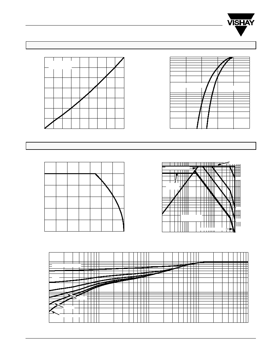
TYPICAL CHARACTERISTICS (25_C UNLESS NOTED)
0.0
0.3
0.6
0.9
1.2
1.5
0.6
0.8
1.0
1.2
1.4
1.6
1.8
2.0
-50 -25
0
25
50
75
100 125 150 175
On-Resistance vs. Junction Temperature
Source-Drain Diode Forward Voltage
(Normalized)
-
On-Resistance (
T
J
- Junction Temperature (
_
C)
V
SD
- Source-to-Drain Voltage (V)
r DS(on)
W
)
-
Source Current (A)
I S
100
10
1
V
GS
= 10 V
I
D
= 17 A
T
J
= 25
_
C
T
J
= 150
_
C
THERMAL RATINGS
1.00
10.00
100.00
0.1
1.0
10.0
100.0
Safe Operating Area
0
10
20
30
40
50
60
0
25
50
75
100
125
150
175
Normalized Thermal Transient Impedance, Junction-to-Case
Square Wave Pulse Duration (sec)
2
1
0.1
0.01
10
-4
10
-3
10
-2
10
-1
Normalized Ef
fective
T
ransient
Thermal Impedance
1
Maximum Avalanche and Drain Current
vs. Case Temperature
T
C
- Case Temperature (
_
C)
V
DS
- Drain-to-Source Voltage (V)
-
Drain Current (A)
ID
-
Drain Current (A)
ID
0.2
0.1
0.05
0.02
Duty Cycle = 0.5
T
C
= 25
_
C
Single Pulse
Single Pulse
I
DM
Limited
I
D(on)
Limited
BV
DSS
Limited
r
DS(on)
Limited
P(t) = 1
P(t) = 0.1
P(t) = 0.01
P(t) = 0.001
P(t) = 0.0001