FEATURES
D TrenchFETr Power MOSFET
D 175_C Junction Temperature
D New Low Thermal Resistance Package
APPLICATIONS
D Automotive and Industrial
SUM110N06-05L
Vishay Siliconix
New Product
Document Number: 72006
S-32618--Rev. B, 29-Dec-03
www.vishay.com
1
N-Channel 60-V (D-S) 175_C MOSFET
PRODUCT SUMMARY
V
(BR)DSS
(V)
r
DS(on)
(W)
I
D
(A)
60
0.0052 @ V
GS
= 10 V
110
a
60
0.0072 @ V
GS
= 4.5 V
110
a
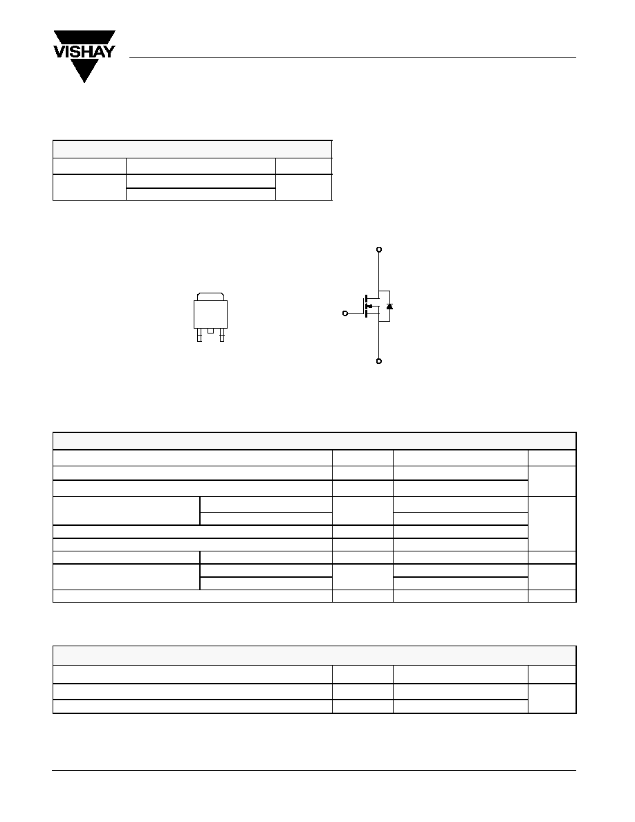
D
G
S
N-Channel MOSFET
TO-263
S
D
G
Top View
Ordering Information: SUM110N06-05L
SUM110N06-05L--E3 (Lead Free)
ABSOLUTE MAXIMUM RATINGS (T
C
= 25_C UNLESS OTHERWISE NOTED)
Parameter
Symbol
Limit
Unit
Drain-Source Voltage
V
DS
60
Gate-Source Voltage
V
GS
"20
V
Continuous Drain Current
(T
J
= 175_C)
T
C
= 25_C
I
D
110
a
Continuous Drain Current
(T
J
= 175_C)
T
C
= 125_C
I
D
82
a
A
Pulsed Drain Current
I
DM
300
A
Avalanche Current
I
AR
75
Repetitive Avalanche Energy
b
L = 0.1 mH
E
AR
280
mJ
Maximum Power Dissipation
b
T
C
= 25_C
P
D
230
c
W
Maximum Power Dissipation
b
T
A
= 25_C
d
P
D
3.75
W
Operating Junction and Storage Temperature Range
T
J
, T
stg
-55 to 175
_C
THERMAL RESISTANCE RATINGS
Parameter
Symbol
Limit
Unit
Junction-to-Ambient--PCB Mount
d
R
thJA
40
_C/W
Junction-to-Case
R
thJC
0.65
_C/W
Notes
a.
Package limited.
b.
Duty cycle v 1%.
c.
See SOA curve for voltage derating.
d.
When mounted on 1" square PCB (FR-4 material).
SUM110N06-05L
Vishay Siliconix
New Product
www.vishay.com
2
Document Number: 72006
S-32618--Rev. B, 29-Dec-03
SPECIFICATIONS (T
J
=25_C UNLESS OTHERWISE NOTED)
Parameter
Symbol
Test Condition
Min
Typ
Max
Unit
Static
Drain-Source Breakdown Voltage
V
(BR)DSS
V
DS
= 0 V, I
D
= 250 mA
60
V
Gate-Threshold Voltage
V
GS(th)
V
DS
= V
GS
, I
D
= 250 mA
1
3
V
Gate-Body Leakage
I
GSS
V
DS
= 0 V, V
GS
= "20 V
"100
nA
V
DS
= 60 V, V
GS
= 0 V
1
Zero Gate Voltage Drain Current
I
DSS
V
DS
= 60 V, V
GS
= 0 V, T
J
= 125_C
50
mA
g
DSS
V
DS
= 60 V, V
GS
= 0 V, T
J
= 175_C
250
m
On-State Drain Current
a
I
D(on)
V
DS
w 5 V, V
GS
= 10 V
120
A
V
GS
= 10 V, I
D
= 30 A
0.0044
0.0052
Drain-Source On-State Resistance
a
r
DS(on)
V
GS
= 4.5 V, I
D
=
20 A
0.0059
0.0072
W
Drain-Source On-State Resistance
a
r
DS(on)
V
GS
= 10 V, I
D
= 30 A, T
J
= 125_C
0.0085
W
V
GS
= 10 V, I
D
= 30 A, T
J
= 175_C
0.011
Forward Transconductance
a
g
fs
V
DS
= 15 V, I
D
= 30 A
30
S
Dynamic
b
Input Capacitance
C
iss
4300
Output Capacitance
C
oss
V
GS
= 0 V, V
DS
= 25 V, f = 1 MHz
770
pF
Reverse Transfer Capacitance
C
rss
365
Total Gate Charge
c
Q
g
80
120
Gate-Source Charge
c
Q
gs
V
DS
= 30 V,
V
GS
= 10 V, I
D
= 110 A
19
nC
Gate-Drain Charge
c
Q
gd
DS
,
GS
,
D
20
Turn-On Delay Time
c
t
d(on)
15
25
Rise Time
c
t
r
V
DD
= 30 V, R
L
= 0.27 W
20
30
ns
Turn-Off Delay Time
c
t
d(off)
V
DD
= 30 V, R
L
= 0.27 W
I
D
^ 110 A, V
GEN
= 10 V, R
g
= 2.5 W
45
70
ns
Fall Time
c
t
f
15
25
Source-Drain Diode Ratings and Characteristics (T
C
= 25_C)
b
Continuous Current
I
S
110
A
Pulsed Current
I
SM
300
A
Forward Voltage
a
V
SD
I
F
= 110 A, V
GS
= 0 V
1.1
1.5
V
Reverse Recovery Time
t
rr
I
110 A di/dt 100 A/
75
125
ns
Peak Reverse Recovery Current
I
RM(REC)
I
F
= 110 A, di/dt = 100 A/ms
2.5
5
A
Reverse Recovery Charge
Q
rr
0.095
0.31
mC
Notes
a.
Pulse test; pulse width v 300 ms, duty cycle v 2%.
b.
Guaranteed by design, not subject to production testing.
c.
Independent of operating temperature.
SUM110N06-05L
Vishay Siliconix
New Product
Document Number: 72006
S-32618--Rev. B, 29-Dec-03
www.vishay.com
3
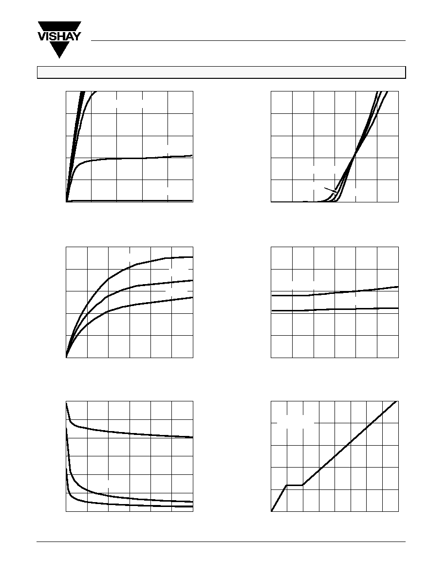
TYPICAL CHARACTERISTICS (25_C UNLESS NOTED)
0
1000
2000
3000
4000
5000
6000
0
10
20
30
40
50
60
0
4
8
12
16
20
0
20
40
60
80
100
120
140
160
0
40
80
120
160
200
0
15
30
45
60
75
90
0.000
0.002
0.004
0.006
0.008
0.010
0
20
40
60
80
100
120
0
50
100
150
200
250
0
1
2
3
4
5
6
0
50
100
150
200
250
0
2
4
6
8
10
Output Characteristics
Transfer Characteristics
Capacitance
Gate Charge
Transconductance
On-Resistance vs. Drain Current
V
DS
- Drain-to-Source Voltage (V)
V
GS
- Gate-to-Source Voltage (V)
-
Drain Current (A)
I
D
-
Gate-to-Source V
oltage (V)
Q
g
- Total Gate Charge (nC)
I
D
- Drain Current (A)
V
DS
- Drain-to-Source Voltage (V)
C
-
Capacitance (pF)
V
GS
-
T
ransconductance
(S)
g
fs
25_C
-55_C
3 V
T
C
= 125_C
V
GS
= 30 V
I
D
= 110 A
V
GS
= 10 thru 5 V
V
GS
= 10 V
C
iss
C
oss
T
C
= -55_C
25_C
125_C
4 V
V
GS
= 4.5 V
-
On-Resistance (
r
DS(on)
W
)
-
Drain Current (A)
I
D
C
rss
I
D
- Drain Current (A)
SUM110N06-05L
Vishay Siliconix
New Product
www.vishay.com
4
Document Number: 72006
S-32618--Rev. B, 29-Dec-03
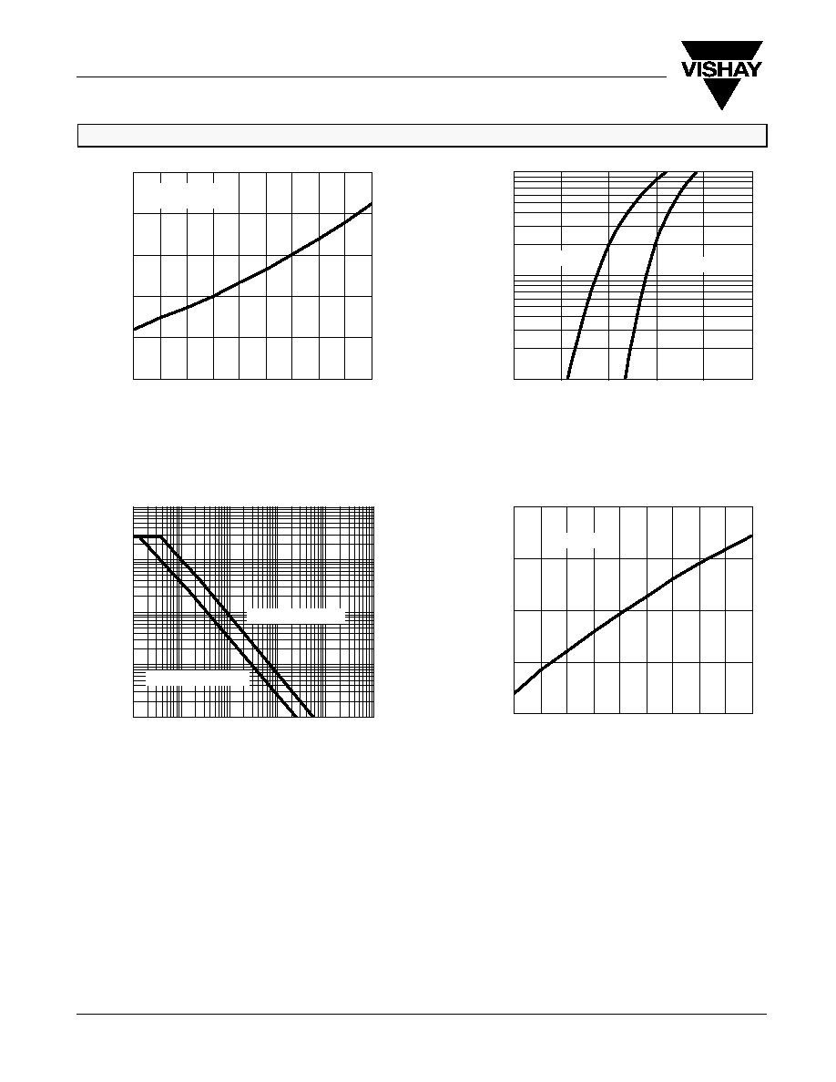
TYPICAL CHARACTERISTICS (25_C UNLESS NOTED)
(Normalized)
-
On-Resistance (
r
DS(on)
W
)
0.0
0.5
1.0
1.5
2.0
2.5
-50 -25
0
25
50
75
100 125 150 175
On-Resistance vs. Junction Temperature
Source-Drain Diode Forward Voltage
T
J
- Junction Temperature (_C)
V
SD
- Source-to-Drain Voltage (V)
-
Source Current (A)
I
S
100
10
1
0.4
0.6
0.8
1.0
1.2
V
GS
= 10 V
I
D
= 110 A
T
J
= 25_C
T
J
= 150_C
0.2
60
65
70
75
80
-50 -25
0
25
50
75
100 125 150 175
Drain Source Breakdown
vs. Junction Temperature
T
J
- Junction Temperature (_C)
I
D
= 10 m A
Avalanche Current vs. Time
t
in
(Sec)
0.00001 0.0001
0.01
1
(a)
I
Dav
0.001
I
AV
(A) @ T
J
= 150_C
0.1
1000
0.1
1
10
100
I
AV
(A) @ T
J
= 25_C
V
(
B
R)
DS
S
(V)
SUM110N06-05L
Vishay Siliconix
New Product
Document Number: 72006
S-32618--Rev. B, 29-Dec-03
www.vishay.com
5
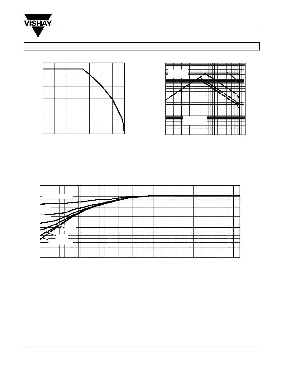
THERMAL RATINGS
0
20
40
60
80
100
120
0
25
50
75
100
125
150
175
Safe Operating Area
V
DS
- Drain-to-Source Voltage (V)
1000
10
0.1
1
10
100
Limited
by r
DS(on)
0.1
100
T
C
= 25_C
Single Pulse
Maximum Drain Current vs.
Case Temperature
T
C
- Ambient Temperature (_C)
-
Drain Current (A)
I
D
1 ms
10 ms
100 ms
dc
10 ms
100 ms
-
Drain Current (A)
I
D
1
Normalized Thermal Transient Impedance, Junction-to-Case
Square Wave Pulse Duration (sec)
2
1
0.1
0.01
10
-4
10
-3
10
-2
10
-1
1
Normalized Ef
fective
T
ransient
Thermal Impedance
10
0.2
0.1
0.05
0.02
Duty Cycle = 0.5
Single Pulse