FEATURES
D
TrenchFET
r
Power MOSFET
D
PWM Optimized for High Efficiency
D
New Low Thermal Resistance PowerPAK
r
Package with Low 1.07-mm Profile
D
100% R
g
Tested
APPLICATIONS
D
Buck Converter
- High Side or Low Side
D
Synchronous Rectifier
- Secondary Rectifier
Si7860ADP
Vishay Siliconix
New Product
Document Number: 72651
S-32674--Rev. A, 29-Dec-03
www.vishay.com
1
N-Channel Reduced Q
g
, Fast Switching MOSFET
PRODUCT SUMMARY
V
DS
(V)
r
DS(on)
(
W
)
I
D
(A)
30
0.0095 @ V
GS
= 10 V
16
30
0.0125 @ V
GS
= 4.5 V
16
1
2
3
4
5
6
7
8
S
S
S
G
D
D
D
D
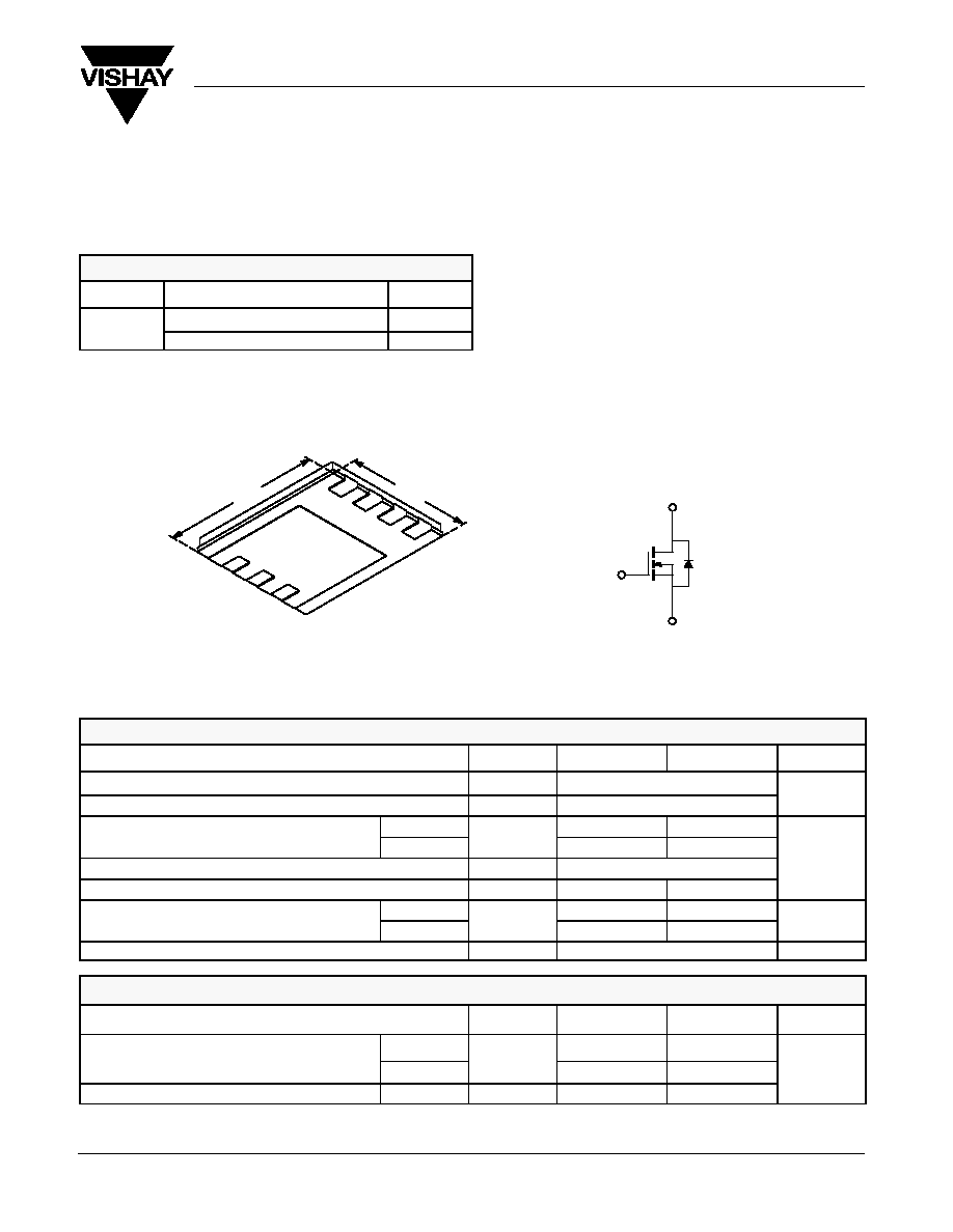
6.15 mm
5.15 mm
PowerPAK SO-8
Bottom View
N-Channel MOSFET
G
D
S
Ordering Information: Si7860ADP-T1-E3
ABSOLUTE MAXIMUM RATINGS (T
A
= 25_C UNLESS OTHERWISE NOTED)
Parameter
Symbol
10 secs
Steady State
Unit
Drain-Source Voltage
V
DS
30
V
Gate-Source Voltage
V
GS
"
20
V
Continuous Drain Current
(T
J
= 150
_
C)
a
T
A
= 25
_
C
I
D
16
11
Continuous Drain Current
(T
J
= 150
_
C)
a
T
A
= 70
_
C
I
D
13
8
A
Pulsed Drain Current
I
DM
"
50
A
Continuous Source Current (Diode Conduction)
a
I
S
4.1
1.5
Maximum Power Dissipation
a
T
A
= 25
_
C
P
D
4.8
1.8
W
Maximum Power Dissipation
a
T
A
= 70
_
C
P
D
3.1
1.1
W
Operating Junction and Storage Temperature Range
T
J
, T
stg
-55 to 150
_
C
THERMAL RESISTANCE RATINGS
Parameter
Symbol
Typical
Maximum
Unit
Maximum Junction to Ambient (MOSFET)
a
t
v
10 sec
R
21
26
Maximum Junction-to-Ambient (MOSFET)
a
Steady State
R
thJA
56
70
_
C/W
Maximum Junction-to-Case (Drain)
Steady State
R
thJC
1.9
2.5
C/W
Notes
a.
Surface Mounted on 1" x 1" FR4 Board.
Si7860ADP
Vishay Siliconix
New Product
www.vishay.com
2
Document Number: 72651
S-32674--Rev. A, 29-Dec-03
MOSFET SPECIFICATIONS (T
J
= 25_C UNLESS OTHERWISE NOTED)
Parameter
Symbol
Test Condition
Min
Typ
Max
Unit
Static
Gate Threshold Voltage
V
GS(th)
V
DS
= V
GS
, I
D
= 250
m
A
1.0
3.0
V
Gate-Body Leakage
I
GSS
V
DS
= 0 V, V
GS
=
"
20 V
"
100
nA
Zero Gate Voltage Drain Current
I
DSS
V
DS
= 30 V, V
GS
= 0 V
1
m
A
Zero Gate Voltage Drain Current
I
DSS
V
DS
= 30 V, V
GS
= 0 V, T
J
= 70
_
C
5
m
A
On-State Drain Current
a
I
D(on)
V
DS
w
5 V, V
GS
= 10
V
40
A
Drain-Source On-State Resistance
a
r
DS(on)
V
GS
= 10
V, I
D
= 16 A
0.0079
0.0095
W
Drain-Source On-State Resistance
a
r
DS(on)
V
GS
= 4.5 V, I
D
= 14 A
0.0105
0.0125
W
Forward Transconductance
a
g
fs
V
DS
= 15 V, I
D
= 16 A
60
S
Diode Forward Voltage
a
V
SD
I
S
= 3 A, V
GS
= 0 V
0.70
1.1
V
Dynamic
b
Total Gate Charge
Q
g
13
18
Gate-Source Charge
Q
gs
V
DS
= 15 V,
V
GS
= 4.5 V, I
D
= 16 A
5
nC
Gate-Drain Charge
Q
gd
4.0
Gate-Resistance
R
g
0.5
1.7
3.2
W
Turn-On Delay Time
t
d(on)
18
27
Rise Time
t
r
V
DD
= 15 V, R
L
= 15
W
12
18
Turn-Off Delay Time
t
d(off)
V
DD
= 15 V, R
L
= 15
W
I
D
^
1 A, V
GEN
= 10 V, R
G
= 6
W
46
70
ns
Fall Time
t
f
19
30
Source-Drain Reverse Recovery Time
t
rr
I
F
= 3 A, di/dt = 100 A/
m
s
40
70
Notes
a.
Pulse test; pulse width
v
300
m
s, duty cycle
v
2%.
b.
Guaranteed by design, not subject to production testing.
TYPICAL CHARACTERISTICS (25_C UNLESS NOTED)
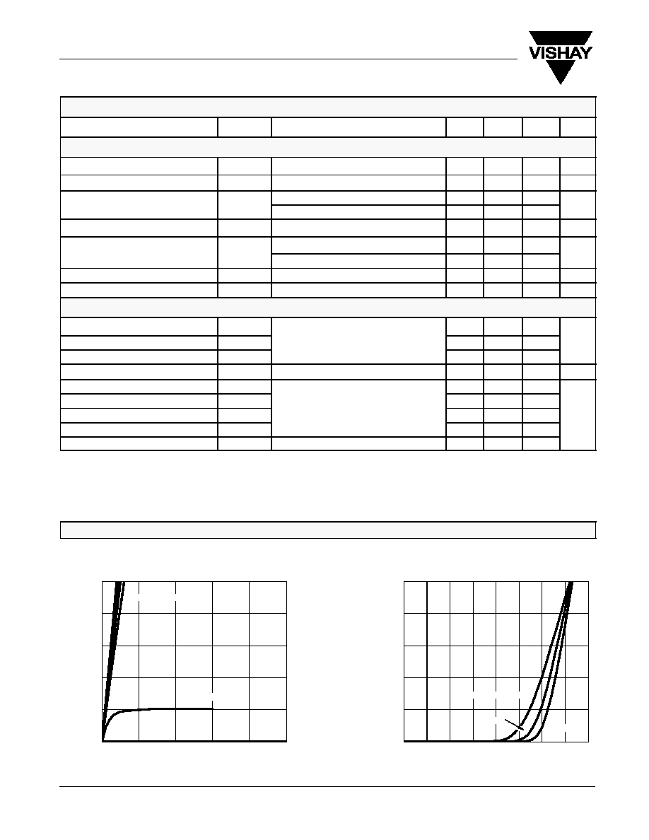
0
10
20
30
40
50
0.0
0.5
1.0
1.5
2.0
2.5
3.0
3.5
4.0
0
10
20
30
40
50
0
1
2
3
4
5
V
GS
= 10 thru 4 V
25
_
C
T
C
= 125
_
C
-55
_
C
3 V
Output Characteristics
Transfer Characteristics
V
DS
- Drain-to-Source Voltage (V)
-
Drain Current (A)
I
D
V
GS
- Gate-to-Source Voltage (V)
-
Drain Current (A)
I
D
Si7860ADP
Vishay Siliconix
New Product
Document Number: 72651
S-32674--Rev. A, 29-Dec-03
www.vishay.com
3
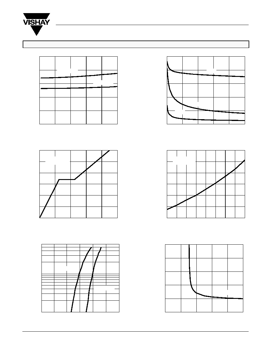
TYPICAL CHARACTERISTICS (25_C UNLESS NOTED)
0.000
0.003
0.006
0.009
0.012
0.015
0
10
20
30
40
50
0
1
2
3
4
5
6
0
4
8
12
16
20
0.50
0.75
1.00
1.25
1.50
1.75
2.00
-50
-25
0
25
50
75
100
125
150
0
500
1000
1500
2000
2500
0
6
12
18
24
30
C
rss
C
oss
C
iss
V
DS
= 15 V
I
D
= 16 A
V
GS
= 10 V
I
D
= 16 A
V
GS
= 10 V
Gate Charge
On-Resistance vs. Drain Current
-
Gate-to-Source V
oltage (V)
Q
g
- Total Gate Charge (nC)
V
DS
- Drain-to-Source Voltage (V)
C
-
Capacitance (pF)
V
GS
-
On-Resistance (
r
DS(on)
W
)
I
D
- Drain Current (A)
Capacitance
On-Resistance vs. Junction Temperature
T
J
- Junction Temperature (
_
C)
(Normalized)
-
On-Resistance (
r
DS(on)
W
)
V
GS
= 4.5 V
1.0
1.2
0.000
0.008
0.016
0.024
0.032
0.040
0
2
4
6
8
10
1
10
60
I
D
= 16 A
0.00
0.2
0.4
0.6
0.8
T
J
= 25
_
C
T
J
= 150
_
C
Source-Drain Diode Forward Voltage
On-Resistance vs. Gate-to-Source Voltage
-
On-Resistance (
r
DS(on)
W
)
V
SD
- Source-to-Drain Voltage (V)
V
GS
- Gate-to-Source Voltage (V)
-
Source Current (A)
I
S
Si7860ADP
Vishay Siliconix
New Product
www.vishay.com
4
Document Number: 72651
S-32674--Rev. A, 29-Dec-03
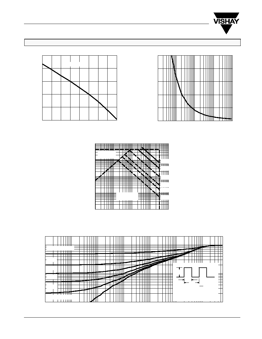
TYPICAL CHARACTERISTICS (25_C UNLESS NOTED)
-0.9
-0.6
-0.3
0.0
0.3
0.6
-50
-25
0
25
50
75
100
125
150
I
D
= 250
m
A
Threshold Voltage
V
ariance (V)
V
GS(th)
T
J
- Temperature (
_
C)
10
-3
10
-2
1
10
600
10
-1
10
-4
100
0.001
0
1
160
200
40
10
0.01
Single Pulse Power, Juncion-To-Ambient
Time (sec)
120
80
Power (W)
2
1
0.1
0.01
0.2
0.1
0.05
0.02
Single Pulse
Duty Cycle = 0.5
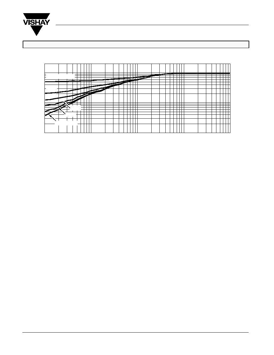
Normalized Thermal Transient Impedance, Junction-to-Ambient
Square Wave Pulse Duration (sec)
Normalized Ef
fective
T
ransient
Thermal Impedance
1. Duty Cycle, D =
2. Per Unit Base = R
thJA
= 125
_
C/W
3. T
JM
- T
A
= P
DM
Z
thJA(t)
t
1
t
2
t
1
t
2
Notes:
4. Surface Mounted
P
DM
0.1
Safe Operating Area, Junction-to-Case
V
DS
- Drain-to-Source Voltage (V)
100
1
0.01
1
10
100
0.01
10
-
Drain Current (A)
I
D
0.1
0.1
Limited by
r
DS(on)
T
C
= 25
_
C
Single Pulse
10 ms
100 ms
dc
1 s
10 s
1 ms
Si7860ADP
Vishay Siliconix
New Product
Document Number: 72651
S-32674--Rev. A, 29-Dec-03
www.vishay.com
5
TYPICAL CHARACTERISTICS (25_C UNLESS NOTED)
10
-3
10
-2
1
10
-1
10
-4
2
1
0.1
0.01
0.2
0.1
0.05
0.02
Single Pulse
Duty Cycle = 0.5
Normalized Thermal Transient Impedance, Junction-to-Case
Square Wave Pulse Duration (sec)
Normalized Ef
fective
T
ransient
Thermal Impedance