Vishay Siliconix
SPICE Device Model SUR50N024-06P
N-Channel 20-V (D-S) 175
∞ MOSFET
CHARACTERISTICS
∑ N-Channel Vertical DMOS
∑ Macro Model (Subcircuit Model)
∑ Level 3 MOS
∑ Apply for both Linear and Switching Application
∑ Accurate over the -55 to 125∞C Temperature Range
∑ Model the Gate Charge, Transient, and Diode Reverse Recovery
Characteristics
DESCRIPTION
The attached spice model describes the typical electrical
characteristics of the n-channel vertical DMOS. The subcircuit
model is extracted and optimized over the
-55 to 125∞C
temperature ranges under the pulsed 0-V to 10-V gate drive. The
saturated output impedance is best fit at the gate bias near the
threshold voltage.
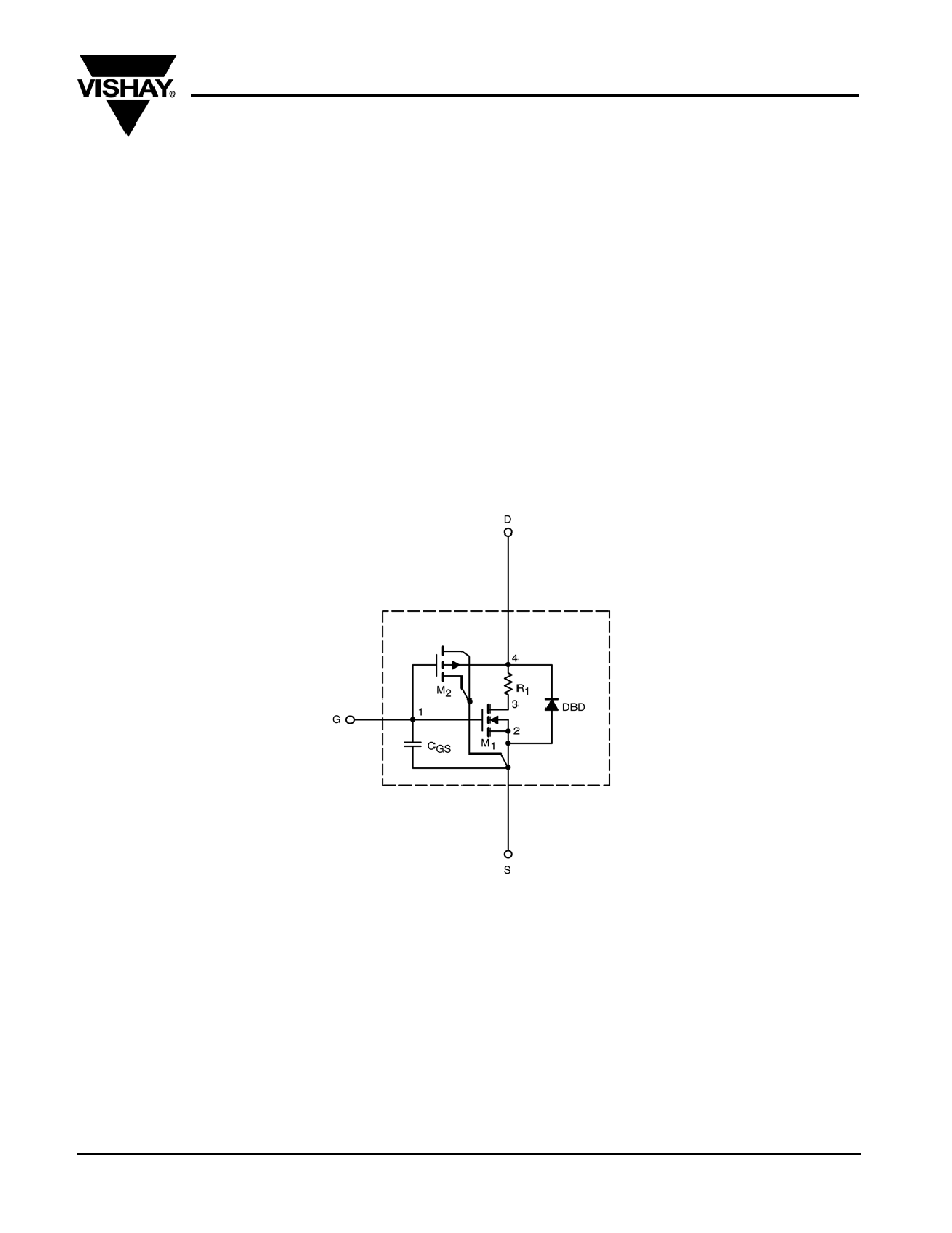
A novel gate-to-drain feedback capacitance network is used to model
the gate charge characteristics while avoiding convergence difficulties
of the switched C
gd
model. All model parameter values are optimized
to provide a best fit to the measured electrical data and are not
intended as an exact physical interpretation of the device.
SUBCIRCUIT MODEL SCHEMATIC
This document is intended as a SPICE modeling guideline and does not constitute a commercial product data sheet. Designers should refer to the appropriate
data sheet of the same number for guaranteed specification limits.
1
www.vishay.com
Document Number: 73019
S-60245
Rev. B, 20-Feb-06
Vishay Siliconix
SPICE Device Model SUR50N024-06P
SPECIFICATIONS (T
J
= 25
∞C UNLESS OTHERWISE NOTED)
Parameter Symbol
Test
Condition
Simulated
Data
Measured
Data
Unit
Static
Gate Threshold Voltage
V
GS(th)
V
DS
= V
GS
, I
D
= 250
µA
1.4 V
On-State Drain Current
a
I
D(on)
V
DS
= 5 V, V
GS
= 10 V
964
A
V
GS
= 10 V, I
D
= 20 A
0.0041
0.0046
V
GS
= 10 V, I
D
= 20 A, T
J
= 125
∞C
0.0057
Drain-Source On-State Resistance
a
r
DS(on)
V
GS
= 4.5 V, I
D
= 20 A
0.0065
0.0073
Forward Voltage
a
V
SD
I
S
= 50 A, V
GS
= 0 V
0.91
1.2
V
Dynamic
b
Input Capacitance
C
iss
2418
2550
Output Capacitance
C
oss
816
900
Reverse Transfer Capacitance
C
rss
V
GS
= 0 V, V
DS
= 10 V, f = 1 MHz
348 415
pF
Total Gate Charge
c
Q
g
20
19
Gate-Source Charge
c
Q
gs
7.5
7.5
Gate-Drain Charge
c
Q
gd
V
DS
= 10 V, V
GS
= 4.5 V, I
D
= 50 A
6 6
nC
Turn-On Delay Time
c
t
d(on)
11
11
Rise Time
c
t
r
10
10
Turn-Off Delay Time
c
t
d(off)
9
24
Fall Time
c
t
f
V
DD
= 10 V, R
L
= 0.20
I
D
50 A, V
GEN
= 10 V, R
G
= 2.5
9 9
Source-Drain Reverse Recovery Time
t
rr
I
F
= 50 A, di/dt = 100 A/
µs
31 35
ns
Notes
a. Pulse test; pulse width
300 µs, duty cycle 2%.
b. Guaranteed by design, not subject to production testing.
c. Independent of operating temperature.
2
www.vishay.com
Document Number: 73019
S-60245
Rev. B, 20-Feb-06
Vishay Siliconix
SPICE Device Model SUR50N024-06P
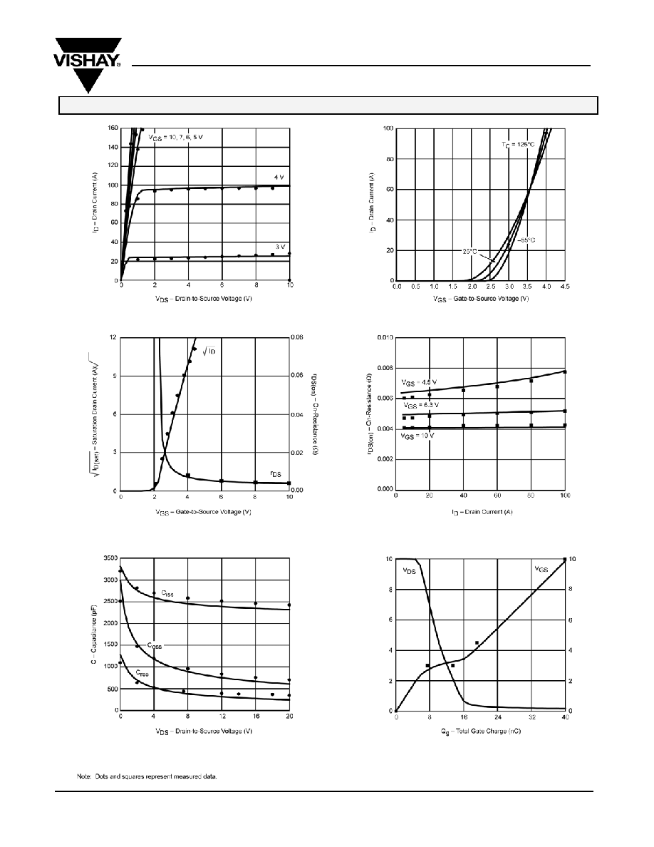
COMPARISON OF MODEL WITH MEASURED DATA (T
J
=25
∞C UNLESS OTHERWISE NOTED)
3
www.vishay.com
Document Number: 73019
S-60245
Rev. B, 20-Feb-06