 | –≠–ª–µ–∫—Ç—Ä–æ–Ω–Ω—ã–π –∫–æ–º–ø–æ–Ω–µ–Ω—Ç: TCET1202G | –°–∫–∞—á–∞—Ç—å:  PDF PDF  ZIP ZIP |

TCET1200/ TCET1200G/ TCET2200
Document Number 83501
Rev. 1.5, 26-Oct-04
Vishay Semiconductors
www.vishay.com
1
E
A
C
8 PIN
C
4 PIN
15123
C
V
D E
1
2
3
4
Pb
Pb-free
e3
Optocoupler, Phototransistor Output (Single, Dual Channel)
Features
∑ Extra low coupling capacity - typical 0.2 pF
∑ High Common Mode Rejection
∑ CTR offered in 5 groups
∑ Low temperature coefficient of CTR
∑ Available in single or dual channel
∑ Lead-free component
∑ Component in accordance to RoHS 2002/95/EC
and WEEE 2002/96/EC
Agency Approvals
∑ UL1577, File No. E76222 System Code U, Double
Protection
∑ CSA 22.2 bulletin 5A, Double Protection
∑ BSI IEC60950 IEC60065
∑ DIN EN 60747-5-2 (VDE0884)
DIN EN 60747-5-5 pending
∑ FIMKO
Applications
Switch-mode power supplies
Line receiver
Computer peripheral interface
Microprocessor system interface
Reinforced Isolation provides circuit protection
against electrical shock (Safety Class II)
Circuits for safe protective separation against electri-
cal shock according to safety class II (reinforced iso-
lation):
∑ For appl. class I - IV at mains voltage
300 V
∑ For appl. class I - III at mains voltage
600 V accord-
ing to DIN EN 60747-5-2(VDE0884)/ DIN EN 60747-
5-5 pending, table 2, suitable for:
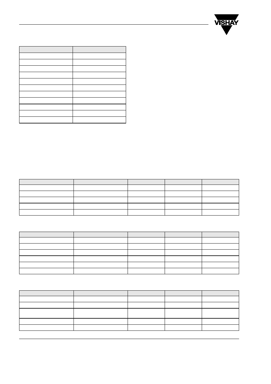
Description
The TCET1200/ TCET2200 consists of a phototrans-
istor optically coupled to a gallium arsenide infrared-
emitting diode in a 4-pin (single channel) or 8-pin
plastic dual inline package.
VDE Standards
These couplers perform safety functions according to the following
equipment standards:
DIN EN 60747-5-2(VDE0884)/ DIN EN 60747-5-5
pending
Optocoupler for electrical safety requirements
IEC 60950/EN 60950
Office machines (applied for reinforced isolation for mains voltage
400 VRMS)
VDE 0804
Telecommunication apparatus and data processing
IEC 60065
Safety for mains-operated electronic and related household appa-
ratus
www.vishay.com
2
Document Number 83501
Rev. 1.5, 26-Oct-04
TCET1200/ TCET1200G/ TCET2200
Vishay Semiconductors
Order Information
G = Leadform 10.16 mm; G is not marked on the body
Absolute Maximum Ratings
T
amb
= 25 ∞C, unless otherwise specified
Stresses in excess of the absolute Maximum Ratings can cause permanent damage to the device. Functional operation of the device is
not implied at these or any other conditions in excess of those given in the operational sections of this document. Exposure to absolute
Maximum Rating for extended periods of the time can adversely affect reliability.
Input
Output
Coupler
Part
Remarks
TCET1200
CTR 50 - 600 %, DIP-4
TCET1201
CTR 40 - 80 %, DIP-4
TCET2200
CTR 50 - 600 %, DIP-8
TCET1202
CTR 63 - 125 %, DIP-4
TCET1203
CTR 100 - 200 %, DIP-4
TCET1204
CTR 160 - 320 %, DIP-4
TCET1200G
CTR 50 - 600 %, DIP-4
TCET1201G
CTR 40 - 80 %, DIP-4
TCET1202G
CTR 63 - 125 %, DIP-4
TCET1203G
CTR 100 - 200 %, DIP-4
TCET1204G
CTR 160 - 320 %, DIP-4
Parameter
Test condition
Symbol
Value
Unit
Reverse voltage
V
R
6
V
Forward current
I
F
60
mA
Forward surge current
t
p
10 µs
I
FSM
1.5
A
Power dissipation
P
diss
100
mW
Junction temperature
T
j
125
∞C
Parameter
Test condition
Symbol
Value
Unit
Collector emitter voltage
V
CEO
70
V
Emitter collector voltage
V
ECO
7
V
Collector current
I
C
50
mA
Collector peak current
t
p
/T = 0.5, t
p
10 ms
I
CM
100
mA
Power dissipation
P
diss
150
mW
Junction temperature
T
j
125
∞C
Parameter
Test condition
Symbol
Value
Unit
Isolation test voltage (RMS)
V
ISO
5000
V
RMS
Total power dissipation
P
tot
250
mW
Operating ambient temperature
range
T
amb
- 40 to + 100
∞C
Storage temperature range
T
stg
- 55 to + 125
∞C
Soldering temperature
2 mm from case t
10 s
T
sld
260
∞C
TCET1200/ TCET1200G/ TCET2200
Document Number 83501
Rev. 1.5, 26-Oct-04
Vishay Semiconductors
www.vishay.com
3
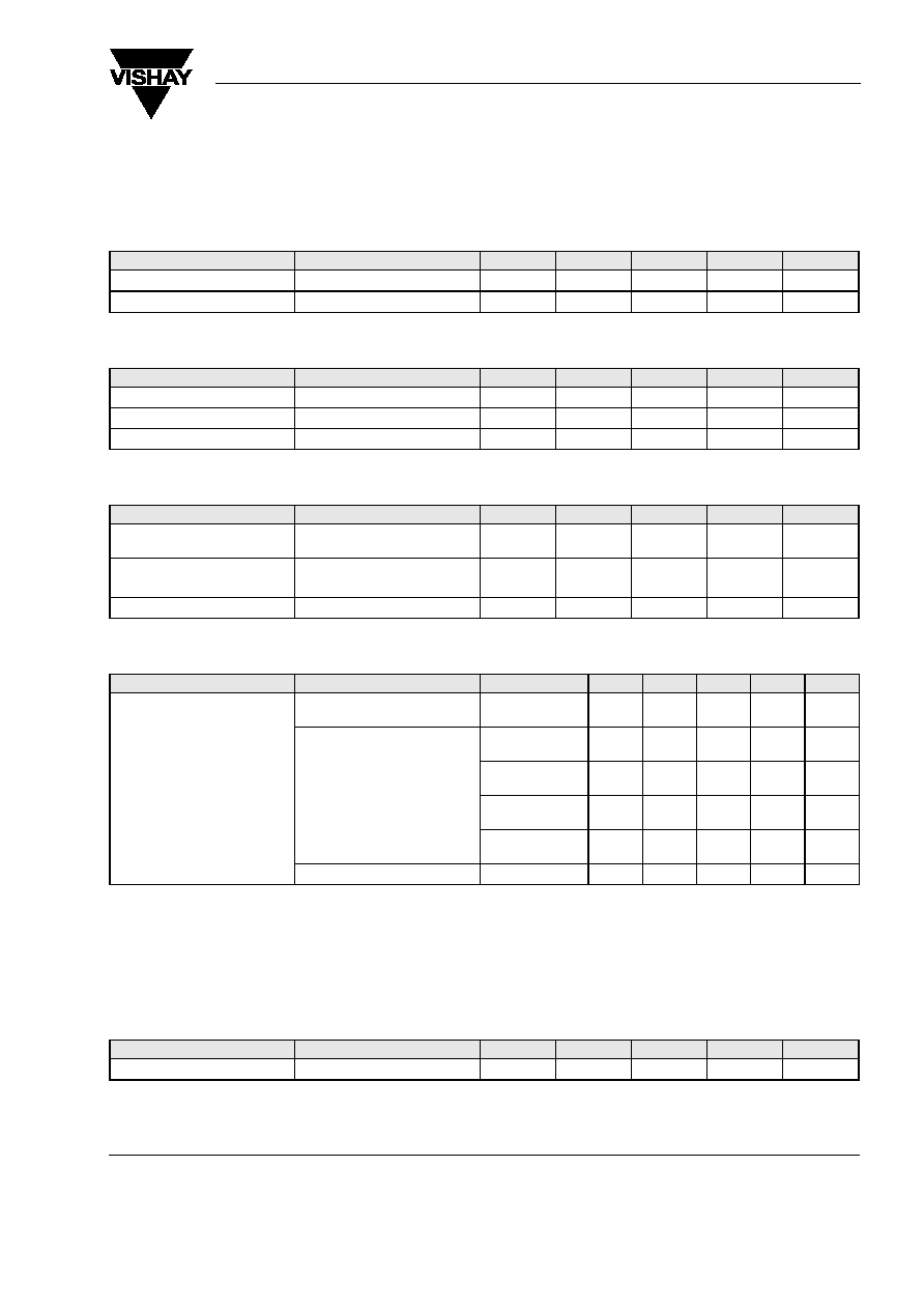
Electrical Characteristics
T
amb
= 25 ∞C, unless otherwise specified
Minimum and maximum values are testing requirements. Typical values are characteristics of the device and are the result of engineering
evaluation. Typical values are for information only and are not part of the testing requirements.
Input
Output
Coupler
Current Transfer Ratio
Maximum Safety Ratings
(according to DIN EN 60747-5-2(VDE0884)/ DIN EN 60747-5-5 pending) see figure 1
This optocoupler is suitable for safe electrical isolation only within the safety ratings.
Compliance with the safety ratings shall be ensured by means of suitable protective circuits.
Input
Parameter
Test condition
Symbol
Min
Typ.
Max
Unit
Forward voltage
I
F
= ± 50 mA
V
F
1.25
1.6
V
Junction capacitance
V
R
= 0 V, f = 1 MHz
C
j
50
pF
Parameter
Test condition
Symbol
Min
Typ.
Max
Unit
Collector emitter voltage
I
C
= 1 mA
V
CEO
70
V
Emitter collector voltage
I
E
= 100
µA
V
ECO
7
V
Collector-emitter cut-off current
V
CE
= 20 V, I
f
= 0, E = 0
I
CEO
10
100
nA
Parameter
Test condition
Symbol
Min
Typ.
Max
Unit
Collector emitter saturation
voltage
I
F
= 10 mA, I
C
= 1 mA
V
CEsat
0.3
V
Cut-off frequency
V
CE
= 5 V, I
F
= 10 mA,
R
L
= 100
f
c
110
kHz
Coupling capacitance
f = 1 MHz
C
k
0.3
pF
Parameter
Test condition
Part
Symbol
Min
Typ.
Max
Unit
I
C
/I
F
V
CE
= 5 V, I
F
= 5 mA
TCET1200
TCET1200G
CTR
50
600
%
V
CE
= 5 V, I
F
= 10 mA
TCET1201
TCET1201G
CTR
40
80
%
TCET1202
TCET1202G
CTR
63
125
%
TCET1203
TCET1203G
CTR
100
200
%
TCET1204
TCET1204G
CTR
160
320
%
V
CE
= 5 V, I
F
= 5 mA
TCET2200
CTR
50
600
%
Parameter
Test condition
Symbol
Min
Typ.
Max
Unit
Forward current
I
F
130
mA

www.vishay.com
4
Document Number 83501
Rev. 1.5, 26-Oct-04
TCET1200/ TCET1200G/ TCET2200
Vishay Semiconductors
Output
Coupler
Insulation Rated Parameters
Parameter
Test condition
Symbol
Min
Typ.
Max
Unit
Power dissipation
P
diss
265
mW
Parameter
Test condition
Symbol
Min
Typ.
Max
Unit
Rated impulse voltage
V
IOTM
8
kV
Safety temperature
T
si
150
∞C
Parameter
Test condition
Symbol
Min
Typ.
Max
Unit
Partial discharge test voltage -
Routine test
100 %, t
test
= 1 s
V
pd
1.6
kV
Partial discharge test voltage -
Lot test (sample test)
t
Tr
= 60 s, t
test
= 10 s,
(see figure 2)
V
IOTM
8
kV
V
pd
1.3
kV
Insulation resistance
V
IO
= 500 V
R
IO
10
12
V
IO
= 500 V, T
amb
= 100 ∞C
R
IO
10
11
V
IO
= 500 V, T
amb
= 150 ∞C
(construction test only)
R
IO
10
9
Figure 1. Derating diagram
0
25
50
75
125
0
50
100
150
200
300
P
≠
T
otal Power Dissipation ( mW )
tot
T
si
≠ Safety Temperature (
∞C )
150
94 9182
100
250
Phototransistor
Psi ( mW )
IR-Diode
Isi ( mA )
Figure 2. Test pulse diagram for sample test according to DIN EN
60747-5-2(VDE0884)/ DIN EN 60747-; IEC60747
t
13930
t
1
, t
2
= 1 to 10 s
t
3
, t
4
= 1 s
t
test
= 10 s
t
stres
= 12 s
V
IOTM
V
Pd
V
IOWM
V
IORM
0
t
1
t
test
t
Tr
= 60 s
t
stres
t
3
t
4
t
2

TCET1200/ TCET1200G/ TCET2200
Document Number 83501
Rev. 1.5, 26-Oct-04
Vishay Semiconductors
www.vishay.com
5
Switching Characteristics
Parameter
Test condition
Symbol
Min
Typ.
Max
Unit
Delay time
V
S
= 5 V, I
C
= 2 mA, R
L
= 100
(see figure 3)
t
d
3.0
µs
Rise time
V
S
= 5 V, I
C
= 2 mA, R
L
= 100
(see figure 3)
t
r
3.0
µs
Turn-on time
V
S
= 5 V, I
C
= 2 mA, R
L
= 100
(see figure 3)
t
on
6.0
µs
Storage time
V
S
= 5 V, I
C
= 2 mA, R
L
= 100
(see figure 3)
t
s
0.3
µs
Fall time
V
S
= 5 V, I
C
= 2 mA, R
L
= 100
(see figure 3)
t
f
4.7
µs
Turn-off time
V
S
= 5 V, I
C
= 2 mA, R
L
= 100
(see figure 3)
t
off
5.0
µs
Turn-on time
V
S
= 5 V, I
F
= 10 mA, R
L
= 1 k
(see figure 4)
t
on
9.0
µs
Turn-off time
V
S
= 5 V, I
F
= 10 mA, R
L
= 1 k
(see figure 4)
t
off
10.0
µs
Figure 3. Test circuit, non-saturated operation
Figure 4. Test circuit, saturated operation
Channel I
Channel II
95 10804
R
G
= 50
W
t
p
t
p
= 50 s
T
= 0.01
+ 5 V
I
F
0
50
W
100
W
I
F
I
C
= 2 mA; adjusted through
input amplitude
Oscilloscope
R
L
= 1 M
W
C
L
= 20 pF
Channel I
Channel II
95 10843
R
G
= 50
t
p
t
p
= 50 s
T
= 0.01
+ 5 V
I
C
I
F
0
50
1 k
I
F
= 10 mA
Oscilloscope
R
L
C
L
20 pF
M
1
µ
Figure 5. Switching Times
t
p
t
t
0
0
10%
90%
100%
t
r
t
d
t
on
t
s
t
f
t
off
I
F
I
C
96 11698
t
p
pulse duration
t
d
delay time
t
r
rise time
t
on
(= t
d
+ t
r
)
turn-on time
t
s
storage time
t
f
fall time
t
off
(= t
s
+ t
f
)
turn-off time