 | –≠–ª–µ–∫—Ç—Ä–æ–Ω–Ω—ã–π –∫–æ–º–ø–æ–Ω–µ–Ω—Ç: TLMP2100 | –°–∫–∞—á–∞—Ç—å:  PDF PDF  ZIP ZIP |
TLMB / G / O / P / S / Y2100
Document Number 83199
Rev. 1.6, 20-Jan-05
Vishay Semiconductors
www.vishay.com
1
e3 Pb
Pb-free
19226
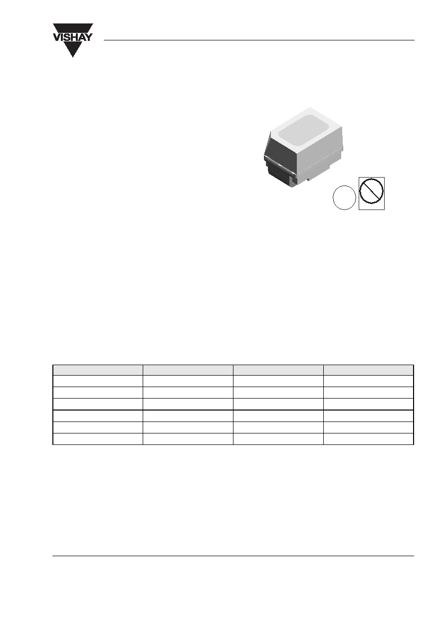
MiniLED
Description
The new MiniLED Series have been designed in a
small white SMT package. The feature of the device
is the very small package 2.3 mm x 1.3 mm x 1.4 mm.
The MinLED is an obvious solution for small-scale,
high-power products that are expected to work reli-
ably in an arduous environment. This is often the case
in automotive and industrial application of course.
Features
∑ SMD LEDs with exceptional brightness
∑ Luminous intensity categorized
∑ Compatible with automatic placement equipment
∑ EIA and ICE standard package
∑ IR reflow soldering
∑ Available in 8 mm tape
∑ Low profile package
∑ Non-diffused lens: excellent for coupling to light
pipes and backlighting
∑ Low power consumption
∑ Luminous intensity ratio in one packaging unit
I
Vmax
/I
Vmin
2.0, optional 1.6
∑ Lead-free device
Applications
Automotive: Backlighting in dashboards and switches
Telecommunication: Indicator and backlighting in
telephone and fax
Indicator and backlight for audio and video equipment
Indicator and backlight in office equipment
Flat backlight for LCDs, switches and symbols
General use
Parts Table
Part
Color, Luminous Intensity
Angle of Half Intensity (±
)
Technology
TLMS2100
Red, I
V
= 7.5 mcd (typ.)
60 ∞
GaAsP on GaP
TLMO2100
Soft orange, I
V
= 7.5 mcd (typ.)
60 ∞
GaAsP on GaP
TLMY2100
Yellow, I
V
= 7.5 mcd (typ.)
60 ∞
GaAsP on GaP
TLMG2100
Green, I
V
= 10 mcd (typ.)
60 ∞
GaP on GaP
TLMP2100
Pure green, I
V
= 2.2 mcd (typ.)
60 ∞
GaP on GaP
TLMB2100
Blue, I
V
= 7 mcd (typ.)
60 ∞
GaN

www.vishay.com
2
Document Number 83199
Rev. 1.6, 20-Jan-05
TLMB / G / O / P / S / Y2100
Vishay Semiconductors
Absolute Maximum Ratings
T
amb
= 25 ∞C, unless otherwise specified
TLMS2100 ,TLMO2100 ,TLMY2100 ,TLMG2100 ,TLMP2100
TLMB2100
Optical and Electrical Characteristics
T
amb
= 25 ∞C, unless otherwise specified
Red
TLMS2100
2)
in one Packing Unit I
Vmax
/I
Vmin
2.0
Parameter
Test condition
Symbol
Value
Unit
Reverse voltage
V
R
6
V
DC Forward current
T
amb
60 ∞C
I
F
30
mA
Surge forward current
t
p
10 µs
I
FSM
0.5
A
Power dissipation
T
amb
60 ∞C
P
V
95
mW
Junction temperature
T
j
100
∞C
Operating temperature range
T
amb
- 40 to + 100
∞C
Storage temperature range
T
stg
- 40 to + 100
∞C
Soldering temperature
according IPC 9501
T
sd
245
∞C
Thermal resistance junction/
ambient
mounted on PC board
(pad size > 5 mm
2
)
R
thJA
480
K/W
Parameter
Test condition
Symbol
Value
Unit
Reverse voltage
V
R
5
V
DC Forward current
T
amb
60 ∞C
I
F
20
mA
Surge forward current
t
p
10 µs
I
FSM
0.1
A
Power dissipation
T
amb
60 ∞C
P
V
90
mW
Junction temperature
T
j
100
∞C
Operating temperature range
T
amb
- 40 to + 100
∞C
Storage temperature range
T
stg
- 40 to + 100
∞C
Soldering temperature
according IPC 9501
T
sd
245
∞C
Thermal resistance junction/
ambient
mounted on PC board
(pad size > 5 mm
2
)
R
thJA
480
K/W
Parameter
Test condition
Symbol
Min
Typ.
Max
Unit
Luminous intensity
2)
I
F
= 10 mA
I
V
2.5
7.5
mcd
Dominant wavelength
I
F
= 10 mA
d
624
628
636
nm
Peak wavelength
I
F
= 10 mA
p
640
nm
Angle of half intensity
I
F
= 10 mA
± 60
deg
Forward voltage
I
F
= 20 mA
V
F
2.1
3.0
V
Reverse voltage
I
R
= 10
µA
V
R
6
15
V
Junction capacitance
V
R
= 0, f = 1 MHz
C
j
15
pF
TLMB / G / O / P / S / Y2100
Document Number 83199
Rev. 1.6, 20-Jan-05
Vishay Semiconductors
www.vishay.com
3
Soft Orange
TLMO2100
2)
in one Packing Unit I
Vmax
/I
Vmin
2.0
Yellow
TLMY2100
2)
in one Packing Unit I
Vmax
/I
Vmin
2.0
Green
TLMG2100
2)
in one Packing Unit I
Vmax
/I
Vmin
2.0
Parameter
Test condition
Symbol
Min
Typ.
Max
Unit
Luminous intensity
2)
I
F
= 10 mA
I
V
3.2
7.5
mcd
Dominant wavelength
I
F
= 10 mA
d
598
605
611
nm
Peak wavelength
I
F
= 10 mA
p
605
nm
Angle of half intensity
I
F
= 10 mA
± 60
deg
Forward voltage
I
F
= 20 mA
V
F
2.1
3
V
Reverse voltage
I
R
= 10
µA
V
R
6
15
V
Junction capacitance
V
R
= 0, f = 1 MHz
C
j
15
pF
Parameter
Test condition
Symbol
Min
Typ.
Max
Unit
Luminous intensity
2)
I
F
= 10 mA
I
V
3.2
7.5
mcd
Dominant wavelength
I
F
= 10 mA
d
581
588
594
nm
Peak wavelength
I
F
= 10 mA
p
585
nm
Angle of half intensity
I
F
= 10 mA
± 60
deg
Forward voltage
I
F
= 20 mA
V
F
2.2
3
V
Reverse voltage
I
R
= 10
µA
V
R
6
15
V
Junction capacitance
V
R
= 0, f = 1 MHz
C
j
15
pF
Parameter
Test condition
Symbol
Min
Typ.
Max
Unit
Luminous intensity
2)
I
F
= 10 mA
I
V
6.3
10
mcd
Dominant wavelength
I
F
= 10 mA
d
562
568
575
nm
Peak wavelength
I
F
= 10 mA
p
565
nm
Angle of half intensity
I
F
= 10 mA
± 60
deg
Forward voltage
I
F
= 20 mA
V
F
2.2
3.0
V
Reverse voltage
I
R
= 10
µA
V
R
6
15
V
Junction capacitance
V
R
= 0, f = 1 MHz
C
j
15
pF
www.vishay.com
4
Document Number 83199
Rev. 1.6, 20-Jan-05
TLMB / G / O / P / S / Y2100
Vishay Semiconductors
Pure green
TLMP2100
2)
in one Packing Unit I
Vmax
/I
Vmin
2.0
Blue
TLMB2100
1)
in one Packing Unit I
Vmax
/I
Vmin
1.6
Typical Characteristics (Tamb = 25
∞C unless otherwise specified)
Parameter
Test condition
Symbol
Min
Typ.
Max
Unit
Luminous intensity
2)
I
F
= 10 mA
I
V
1.0
2.2
mcd
Dominant wavelength
I
F
= 10 mA
d
555
560
565
nm
Peak wavelength
I
F
= 10 mA
p
555
nm
Angle of half intensity
I
F
= 10 mA
± 60
deg
Forward voltage
I
F
= 20 mA
V
F
2.4
3
V
Reverse voltage
I
R
= 10
µA
V
R
6
15
V
Junction capacitance
V
R
= 0, f = 1 MHz
C
j
15
pF
Parameter
Test condition
Symbol
Min
Typ.
Max
Unit
Luminous intensity
1)
I
F
= 10 mA
I
V
4.0
7.0
mcd
Dominant wavelength
I
F
= 10 mA
d
465
nm
Peak wavelength
I
F
= 10 mA
p
428
nm
Angle of half intensity
I
F
= 10 mA
± 60
deg
Forward voltage
I
F
= 20 mA
V
F
3.9
4.5
V
Reverse voltage
I
R
= 10
µA
V
R
5.0
V
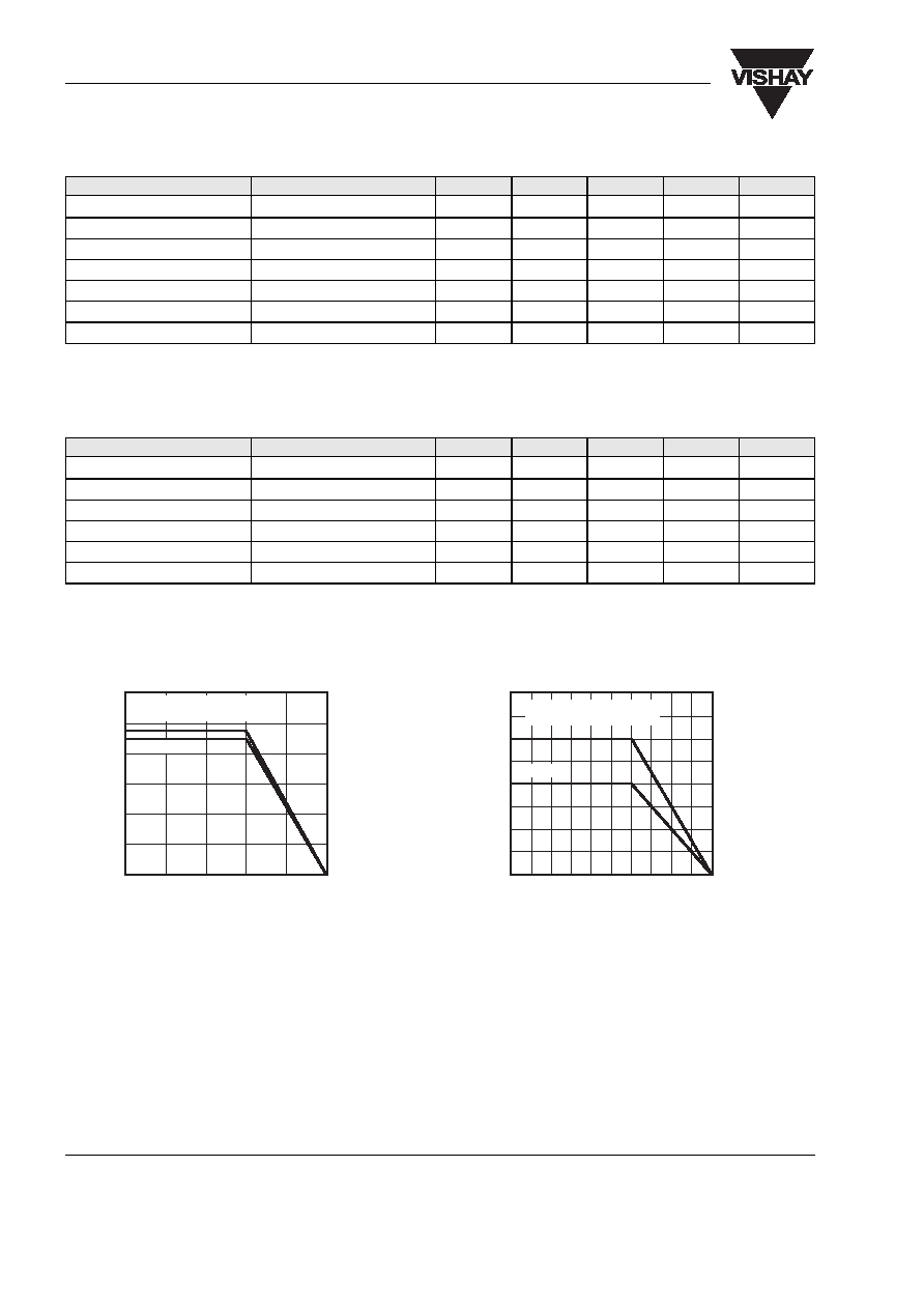
Figure 1. Power Dissipation vs. Ambient Temperature
0
20
40
60
80
100
120
0
20
40
60
80
100
T
amb
- Ambient Temperature (
∞C )
18023
P
-
Power
Dissipation
(mW)
V
Blue
Red, Soft orange,
Yellow, Green, Pure green
Figure 2. Forward Current vs. Ambient Temperature
0
5
10
15
20
25
30
35
40
0
10 20 30 40 50 60 70 80 90 100
T
amb
- Ambient Temperature (
∞C )
18024
I
-
Forward
Current
(
m
A
)
F
Blue
Red, Soft orange,
Yellow, Green, Pure green
TLMB / G / O / P / S / Y2100
Document Number 83199
Rev. 1.6, 20-Jan-05
Vishay Semiconductors
www.vishay.com
5
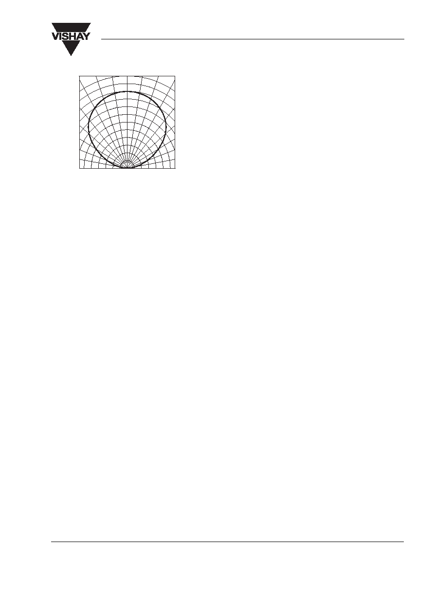
Figure 3. Rel. Luminous Intensity vs. Angular Displacement
0.4
0.2
0
0.2
0.4
0.6
95 10319
0.6
0.9
0.8
0
∞
30
∞
10
∞
20
∞
40
∞
50
∞
60
∞
70
∞
80
∞
0.7
1.0
I
-
Relative
Luminous
Intensity
Vr
e
l