TN2404K/TN2404KL/BS107KL
Vishay Siliconix
Document Number: 72225
S-41761--Rev. B , 04-Oct-04
www.vishay.com
1
N-Channel 240
-V (D-S) MOSFET
PRODUCT SUMMARY
Part Number
V
DS
Min (V)
r
DS(on)
(
W
)
V
GS(th)
(V)
I
D
(A)
Q
g
(Typ)
TN2404K
240
4 @ V
GS
= 10 V
0.8 to 2.0
0.2
4 87
TN2404KL/BS107KL
240
4 @ V
GS
= 10 V
0.8 to 2.0
0.3
4.87
FEATURES
BENEFITS
APPLICATIONS
D Low On-Resistance: 4 W
D Secondary Breakdown Free: 260 V
D Low Power/Voltage Driven
D Low Input and Output Leakage
D Excellent Thermal Stability
D Low Offset Voltage
D Full-Voltage Operation
D Easily Driven Without Buffer
D Low Error Voltage
D No High-Temperature
"Run-Away"
D High-Voltage Drivers: Relays, Solenoids,
Lamps, Hammers, Displays,
Transistors, etc.
D Telephone Mute Switches, Ringer Circuits
D Power Supply, Converters
D Motor Control
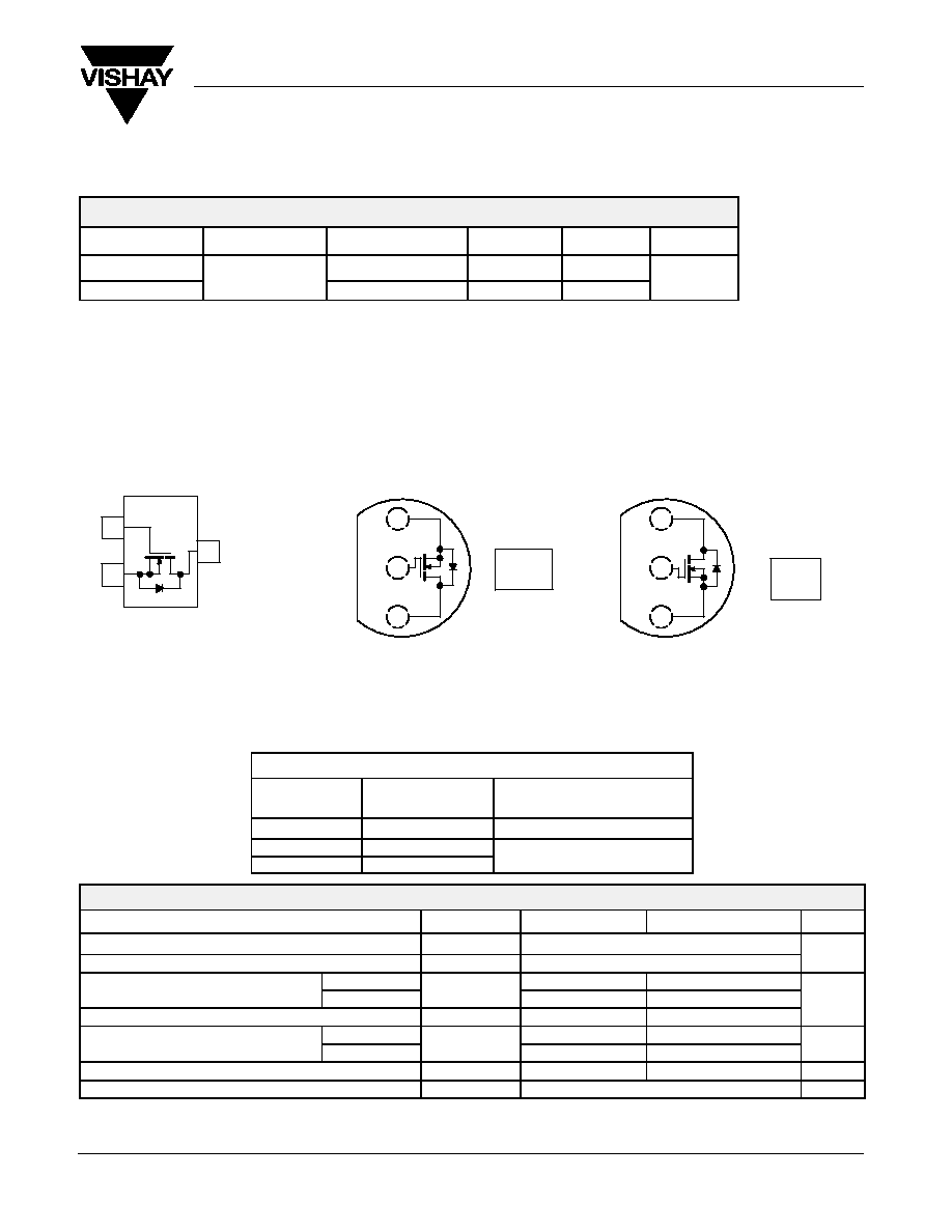
TN2404KL
Device Marking
Front View
"S" TN
2404KL
xxyy
"S" = Siliconix Logo
xxyy
= Date Code
Marking Code: K1
ywl
K1 = Part Number Code for TN2404K
y
= Year Code
w
= Week Code
l
= Lot Traceability
TN2404K
BS107KL
Device Marking
Front View
"S" BS
107KL
xxyy
"S" = Siliconix Logo
xxyy
= Date Code
G
S
D
Top View
2
3
TO-236
(SOT-23)
1
TO-226AA
(TO-92)
Top View
S
D
G
1
2
3
TO-92-18RM
(TO-18 Lead Form)
Top View
D
S
G
1
2
3
ORDERING INFORMATION
Standard
Part Number
Lead (Pb)-Free
Part Number
Option
TN2404K-T1
TN2404K-T1--E3
With Tape and Reel Folding Option
TN2404KL-TR1
TN2404KL-TR1--E3
Spool Option
BS107KL-TR1
BS107KL-TR1--E3
Spool Option
ABSOLUTE MAXIMUM RATINGS (T
A
= 25_C UNLESS OTHERWISE NOTED)
Parameter
Symbol
TN2404K
TN2404KL/BS107KL
Unit
Drain-Source Voltage
V
DS
240
V
Gate-Source Voltage
V
GS
"20
V
Continuous Drain Current
(T
J
= 150_C)
T
A
= 25_C
I
D
0.2
0.3
Continuous Drain Current
(T
J
= 150_C)
T
A
= 70_C
I
D
0.16
0.25
A
Pulsed Drain Current
a
I
DM
0.8
1.4
Power Dissipation
T
A
= 25_C
P
D
0.36
0.8
W
Power Dissipation
T
A
= 70_C
P
D
0.23
0.51
W
Thermal Resistance, Junction-to-Ambient
R
thJA
350
b
156
_C/W
Operating Junction and Storage Temperature Range
T
J
, T
stg
-55 to 150
_C
Notes
a.
Pulse width limited by maximum junction temperature.
b.
Surface mounted on an FR4 board.
TN2404K/TN2404KL/BS107KL
Vishay Siliconix
www.vishay.com
2
Document Number: 72225
S-41761--Rev. B , 04-Oct-04
SPECIFICATIONS (T
A
= 25_C UNLESS OTHERWISE NOTED)
Limits
Parameter
Symbol
Test Conditions
Min
Typ
a
Max
Unit
Static
Drain-Source Breakdown Voltage
V
(BR)DSS
V
GS
= 0 V, I
D
= 100 mA
240
257
V
Gate-Threshold Voltage
V
GS(th)
V
DS
= V
GS
, I
D
= 250 mA
0.8
1.65
2.0
V
Gate-Body Leakage
I
GSS
V
DS
= 0 V, V
GS
= "20 V
"100
nA
Zero Gate Voltage Drain Current
I
DSS
V
DS
= 192 V, V
GS
= 0 V
1
mA
Zero Gate Voltage Drain Current
I
DSS
T
J
= 55_C
10
mA
On State Drain Current
b
I
D( )
V
DS
= 10 V, V
GS
=10 V
0.8
A
On-State Drain Current
b
I
D(on)
V
DS
= 10 V, V
GS
= 4.5 V
0.5
A
V
GS
= 10 V, I
D
= 0.3 A
2.2
4
Drain-Source On-Resistance
b
r
DS(on)
V
GS
= 4.5 V, I
D
= 0.2 A
2.3
4
W
( )
V
GS
= 2.5 V, I
D
= 0.1 A
2.4
6
Forward Transconductance
b
g
fs
V
DS
= 10 V, I
D
= 0.3 A
1.6
S
Diode Forward Voltage
V
SD
I
S
= 0.3 A, V
GS
= 0 V
0.8
1.2
V
Dynamic
a
Total Gate Charge
Q
g
4.87
8
Gate-Source Charge
Q
gs
V
DS
= 192 V, V
GS
= 10 V, I
D
= 0.5 A
0.56
nC
Gate-Drain Charge
Q
gd
1.53
Turn On Time
t
d(on)
5
10
Turn-On Time
t
r
V
DD
= 60 V, R
L
= 200 W
12
20
nS
turn-Off Time
t
d(off)
V
DD
= 60 V, R
L
= 200 W
I
D
] 0.3 A, V
GEN
= 10 V, R
G
= 25 W
35
60
nS
turn-Off Time
t
r
16
25
Notes
a.
For DESIGN AID ONLY, not subject to production testing.
b.
Pulse test: PW v300 ms duty cycle v2%.
Stresses beyond those listed under "Absolute Maximum Ratings" may cause permanent damage to the device. These are stress ratings only, and functional operation
of the device at these or any other conditions beyond those indicated in the operational sections of the specifications is not implied. Exposure to absolute maximum
rating conditions for extended periods may affect device reliability.
TN2404K/TN2404KL/BS107KL
Vishay Siliconix
Document Number: 72225
S-41761--Rev. B , 04-Oct-04
www.vishay.com
3
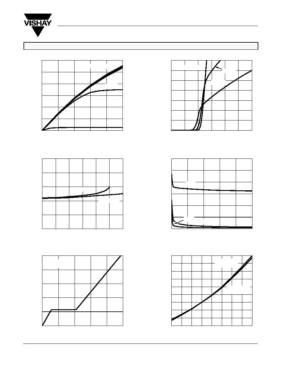
TYPICAL CHARACTERISTICS (25_C UNLESS NOTED)
0
50
100
150
200
250
300
0
10
20
30
40
50
0.0
0.2
0.4
0.6
0.8
1.0
1.2
1.4
0
1
2
3
4
5
6
0.0
0.3
0.6
0.9
1.2
1.5
1.8
0
1
2
3
4
5
V
GS
= 10 thru 3 V
T
C
= -55_C
125_C
25_C
Output Characteristics
Transfer Characteristics
V
DS
- Drain-to-Source Voltage (V)
-
Drain Current (A)
I
D
V
GS
- Gate-to-Source Voltage (V)
-
Drain Current (A)
I
D
2 V
2.5 V
-
On-Resistance (
r
DS(on)
W
)
0.4
0.6
0.8
1.0
1.2
1.4
1.6
1.8
2.0
2.2
-50
-25
0
25
50
75
100
125
150
0
2
4
6
8
10
0
1
2
3
4
5
0
1
2
3
4
5
0.0
0.2
0.4
0.6
0.8
1.0
1.2
V
DS
- Drain-to-Source Voltage (V)
C
rss
C
oss
C
iss
V
DS
= 192 V
I
D
= 0.5 A
I
D
- Drain Current (A)
V
GS
= 4.5 V
I
D
= 0.2 A
V
GS
= 10 V
Gate Charge
On-Resistance vs. Drain Current
-
Gate-to-Source V
oltage (V)
Q
g
- Total Gate Charge (nC)
C
-
Capacitance (pF)
V
GS
Capacitance
On-Resistance vs. Junction Temperature
T
J
- Junction Temperature (_C)
V
GS
= 10 V
I
D
= 0.3 A
V
GS
= 4.5 V
r
DS
(
on)
-
On-Resiistance
(Normalized)
TN2404K/TN2404KL/BS107KL
Vishay Siliconix
www.vishay.com
4
Document Number: 72225
S-41761--Rev. B , 04-Oct-04
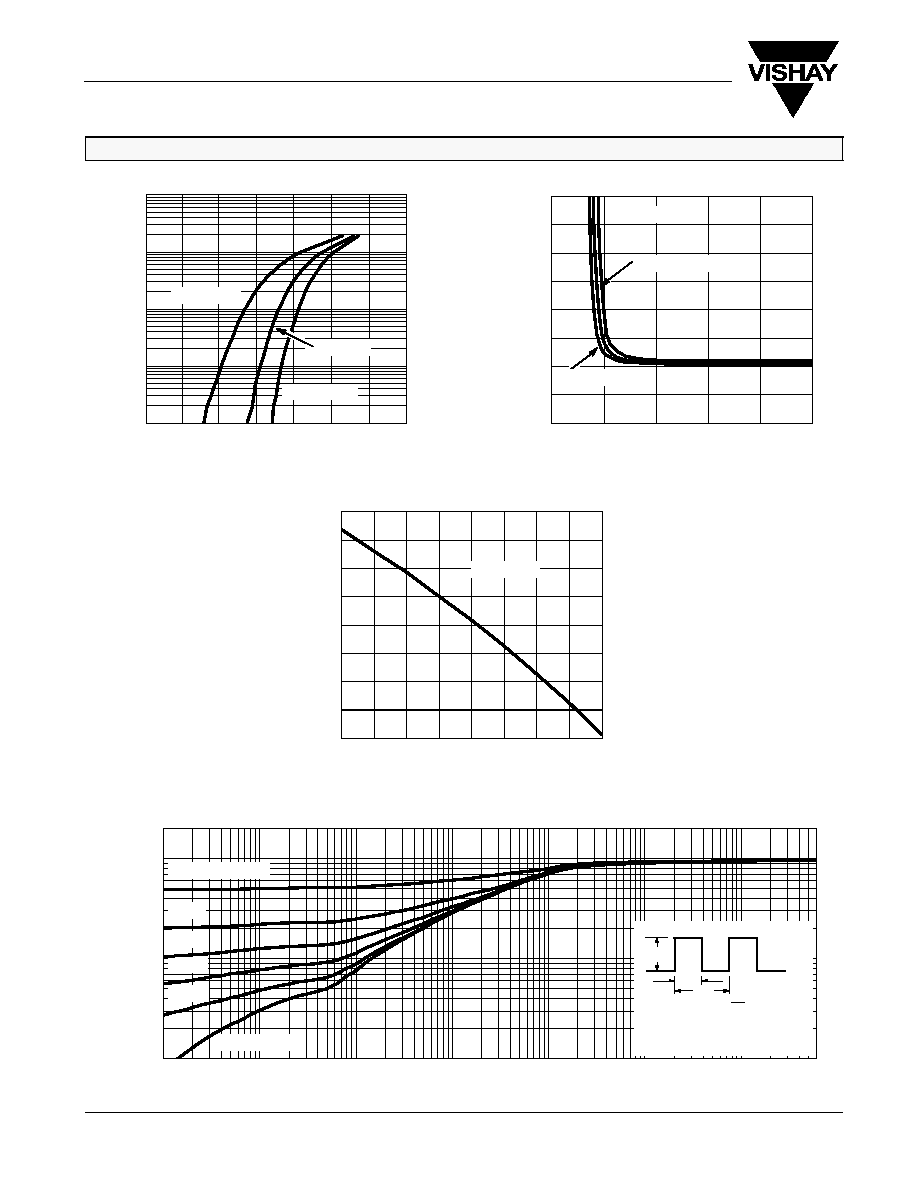
TYPICAL CHARACTERISTICS (25_C UNLESS NOTED)
0.0
0.2
0.4
0.6
0.8
1.0
1.2
1.4
0
1
2
3
4
5
6
7
8
0
2
4
6
8
10
T
J
= 150_C
10
0.001
Source-Drain Diode Forward Voltage
On-Resistance vs. Gate-to-Source Voltage
-
On-Resistance (
r
DS(on)
W
)
V
SD
- Source-to-Drain Voltage (V)
V
GS
- Gate-to-Source Voltage (V)
-
Source Current (A)
I
S
T
J
= 25_C
-0.5
-0.4
-0.3
-0.2
-0.1
-0.0
0.1
0.2
0.3
-50
-25
0
25
50
75
100
125
150
I
D
= 250 mA
Threshold Voltage
V
ariance (V)
V
GS(th)
T
J
- Temperature (_C)
1
0.1
0.01
T
J
= -55_C
I
D
= 50 mA
I
D
= 100 mA
10
-3
10
-2
1
10
600
10
-1
10
-4
100
2
1
0.1
0.01
0.2
0.1
0.05
0.02
Single Pulse
Duty Cycle = 0.5
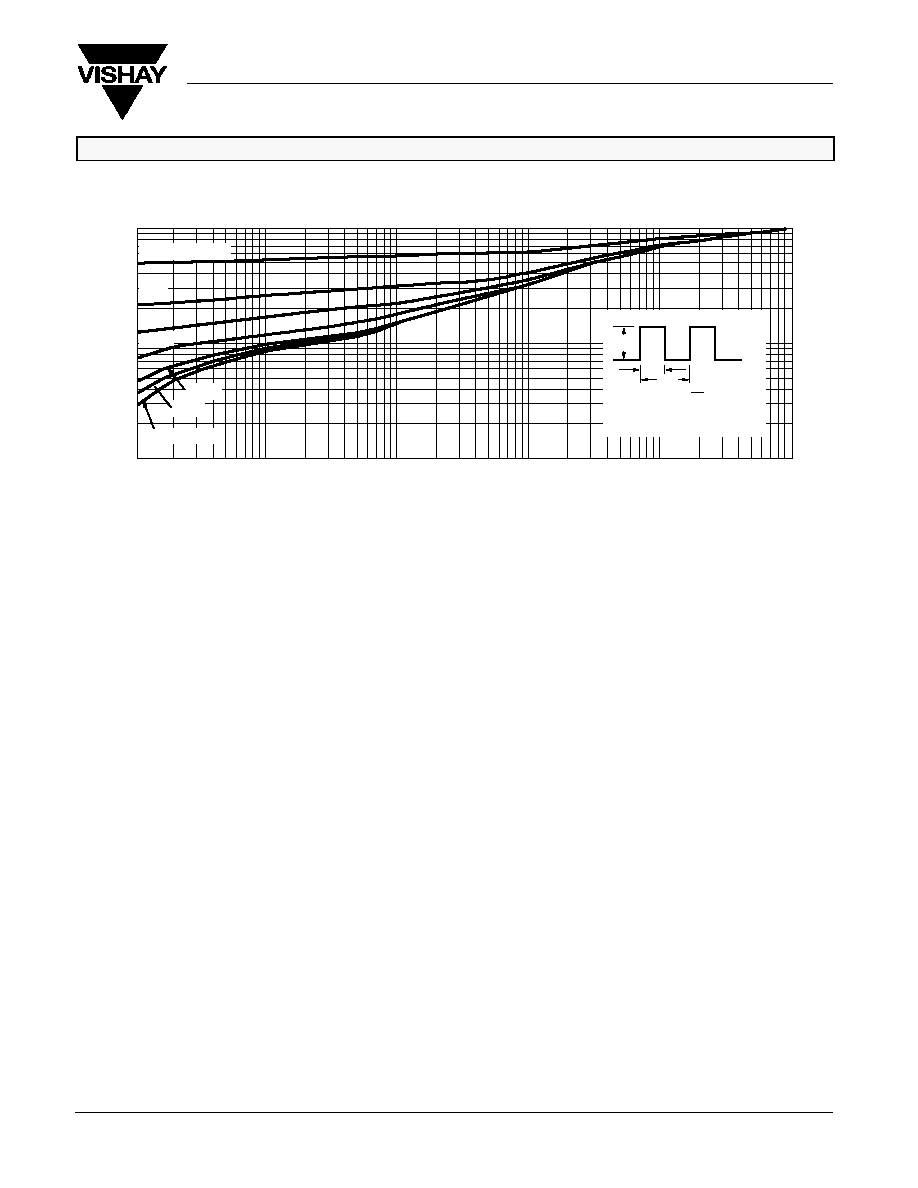
Normalized Thermal Transient Impedance, Junction-to-Ambient (TO-236, TN2404K Only)
Square Wave Pulse Duration (sec)
Normalized Ef
fective
T
ransient
Thermal Impedance
1. Duty Cycle, D =
2. Per Unit Base = R
thJA
=350_C/W
3. T
JM
- T
A
= P
DM
Z
thJA(t)
t
1
t
2
t
1
t
2
Notes:
4. Surface Mounted
P
DM
I
D
= 10 mA
TN2404K/TN2404KL/BS107KL
Vishay Siliconix
Document Number: 72225
S-41761--Rev. B , 04-Oct-04
www.vishay.com
5
TYPICAL CHARACTERISTICS (25_C UNLESS NOTED)
10 K
1
0.01
0.1
0.1
1
100
10
1 K
Duty Cycle = 0.5
0.2
0.1
0.05
0.02
Single Pulse
0.01
Normalized Effective Transient Thermal Impedance, Junction-to-Ambient
(TO-226AA, TN2404KL and TO-92-18RM, BS107KL Only)
Normalized Ef
fecti
ve T
ransient
Thermal Impedance
t
1
- Square Wave Pulse Duration (sec)
1. Duty Cycle, D =
2. Per Unit Base = R
thJA
= 156_C/W
3. T
JM
- T
A
= P
DM
Z
thJA(t)
t
1
t
2
t
1
Notes:
P
DM
t
2
Vishay Siliconix maintains worldwide manufacturing capability. Products may be manufactured at one of several qualified locations. Reliability data for Silicon Technology and
Package Reliability represent a composite of all qualified locations. For related documents such as package/tape drawings, part marking, and reliability data, see
http://www.vishay.com/ppg?72225
.