 | –≠–ª–µ–∫—Ç—Ä–æ–Ω–Ω—ã–π –∫–æ–º–ø–æ–Ω–µ–Ω—Ç: TN2410L | –°–∫–∞—á–∞—Ç—å:  PDF PDF  ZIP ZIP |
TN2410L, VN2406D/L, VN2410L/LS
Vishay Siliconix
Document Number: 70204
S-04279--Rev. F, 16-Jul-01
www.vishay.com
11-1
N-Channel 240-V (D-S) MOSFETs
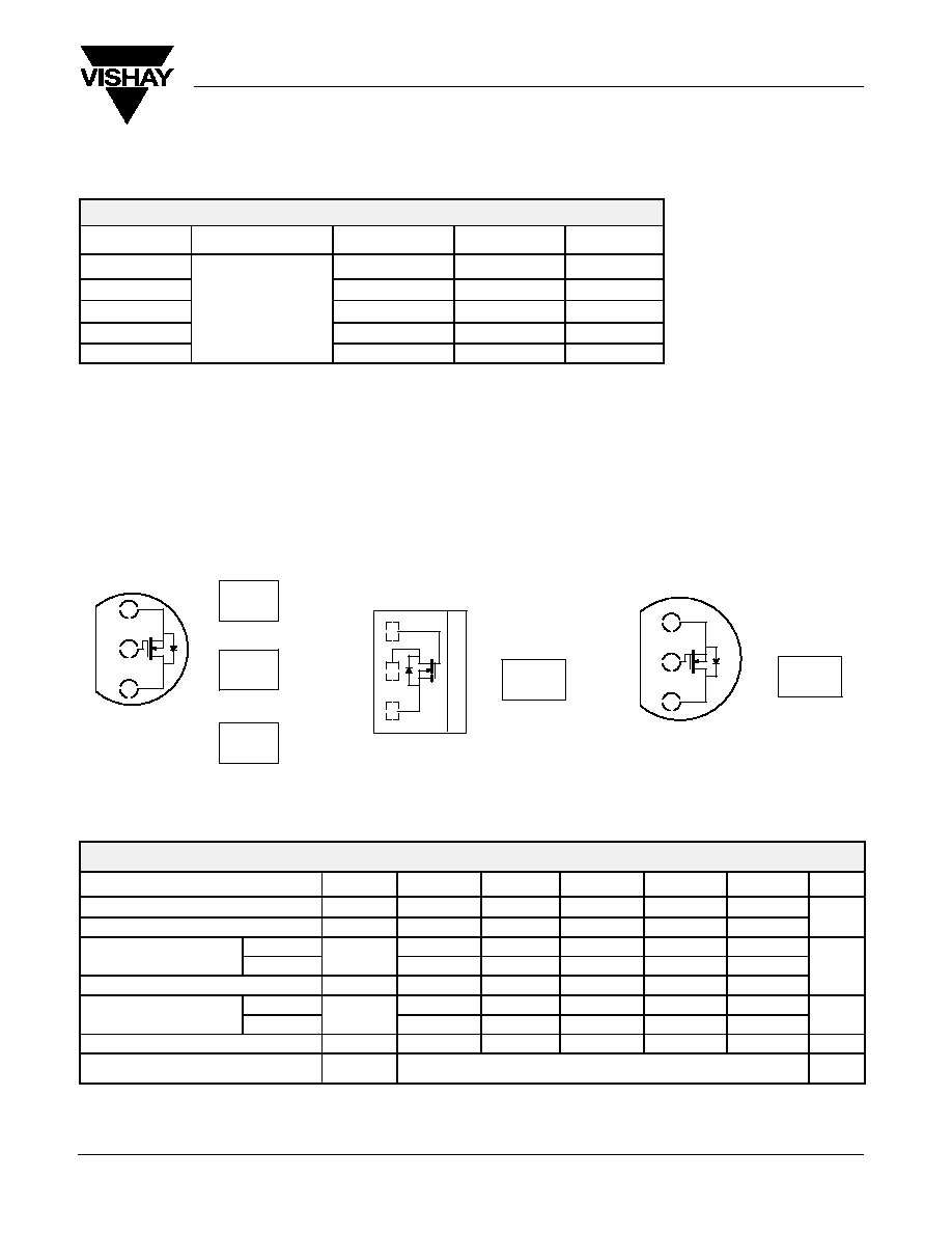
PRODUCT SUMMARY
Part Number
V
(BR)DSS
Min (V)
r
DS(on)
Max (
W
)
V
GS(th)
(V)
I
D
(A)
TN2410L
10 @ V
GS
= 4.5 V
0.5 to 1.8
0.18
VN2406D
6 @ V
GS
= 10 V
0.8 to 2
1.12
VN2406L
240
6
@ V
GS
= 10 V
0.8 to 2
0.18
VN2410L
10 @ V
GS
= 10 V
0.8 to 2
0.18
VN2410LS
10 @ V
GS
= 10 V
0.8 to 2
0.19
FEATURES
BENEFITS
APPLICATIONS
D
Low On-Resistance: 3.5
W
D
Secondary Breakdown Free: 260 V
D
Low Power/Voltage Driven
D
Low Input and Output Leakage
D
Excellent Thermal Stability
D
Low Offset Voltage
D
Full-Voltage Operation
D
Easily Driven Without Buffer
D
Low Error Voltage
D
No High-Temperature "Run-Away"
D
High-Voltage Drivers: Relays, Solenoids, Lamps,
Hammers, Displays, Transistors, etc.
D
Telephone Mute Switches, Ringer Circuits
D
Power Supply, Converters
D
Motor Control
1
TO-220AB
(Tab Drain)
Top View
G
S
D
2
3
TO-226AA
(TO-92)
Top View
S
D
G
1
2
3
TO-92S
(Copper Lead Frame)
Top View
S
D
G
1
2
3
TN2410L
VN2406L
VN2410L
VN2406D
VN2410LS
TN2410L
"S" TN
2410L
xxyy
VN2406L
"S" VN
2406L
xxyy
VN2410L
"S" VN
2410L
xxyy
'Device Marking
Front View
"S" = Siliconix Logo
xxyy = Date Code
VN2406D
"S" xxyy
VN2406D
"S" = Siliconix Logo
xxyy = Date Code
'Device Marking
Front View
'Device Marking
Front View
"S" = Siliconix Logo
xxyy = Date Code
"S" VN
2410LS
xxyy
VN2410LS
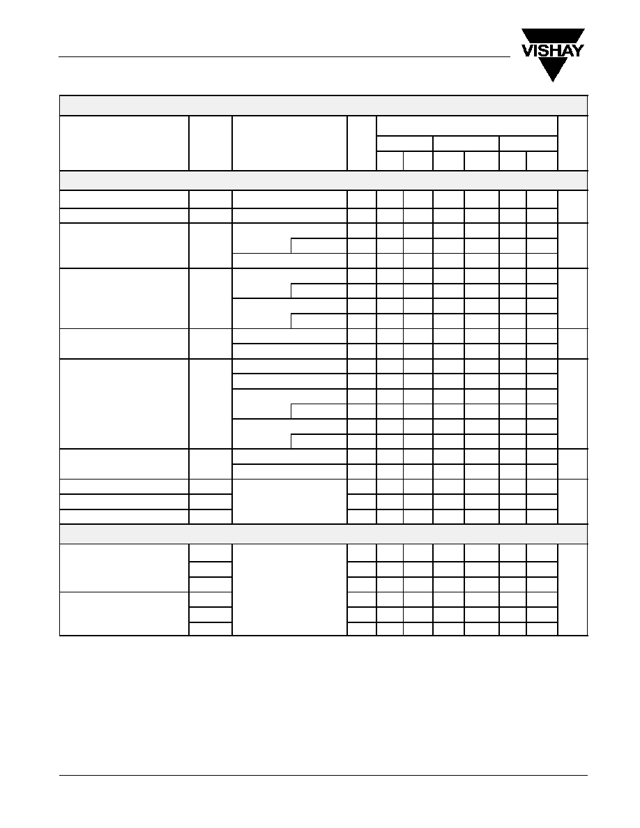
ABSOLUTE MAXIMUM RATINGS (T
A
= 25_C UNLESS OTHERWISE NOTED)
Parameter
Symbol
TN2410L
VN2406D
b
VN2406L
VN2410L
VN2410LS
Unit
Drain-Source Voltage
V
DS
240
240
240
240
240
Gate-Source Voltage
V
GS
"
20
"
20
"
20
"
20
"
20
V
Continuous Drain Current
T
A
= 25
_
C
0.18
1.12
0.18
0.18
0.19
Continuous Drain Current
(T
J
= 150
_
C)
T
A
= 100
_
C
I
D
0.11
0.7
0.11
0.11
0.12
A
Pulsed Drain Current
a
I
DM
1
3
1.7
1.7
2
T
A
= 25
_
C
0.8
20
0.8
0.8
0.9
Power Dissipation
T
A
= 100
_
C
P
D
0.32
8
0.32
0.32
0.4
W
Thermal Resistance, Junction-to-Ambient
R
thJA
156
6.25
c
156
156
139
_
C/W
Operating Junction and
Storage Temperature Range
T
J
, T
stg
≠55 to 150
_
C
Notes
a.
Pulse width limited by maximum junction temperature.
b.
Reference case for all temperature testing.
c.
Maximum junction-to-case
TN2410L, VN2406D/L, VN2410L/LS
Vishay Siliconix
www.vishay.com
11-2
Document Number: 70204
S-04279--Rev. F, 16-Jul-01
SPECIFICATIONS (T
A
= 25_C UNLESS OTHERWISE NOTED)
Limits
TN2410L
VN2406D/L
VN2410L/LS
Parameter
Symbol
Test Conditions
Typ
a
Min
Max
Min
Max
Min
Max
Unit
Static
Drain-Source Breakdown Voltage
V
(BR)DSS
V
GS
= 0 V, I
D
= 100
m
A
260
240
240
240
Gate-Threshold Voltage
V
GS(th)
V
DS
= V
GS
, I
D
= 1 mA
1.4
0.5
1.8
0.8
2
0.8
2
V
V
DS
= 0 V, V
GS
=
"
15 V
"
100
"
100
Gate-Body Leakage
I
GSS
T
J
= 125
_
C
"
500
"
500
nA
V
DS
= 0 V, V
GS
=
"
20 V
"
10
V
DS
= 192 V, V
GS
= 0 V
0.01
1
T
J
= 125
_
C
1
100
m
Zero Gate Voltage Drain Current
I
DSS
V
DS
= 120 V, V
GS
= 0 V
10
10
m
A
T
J
= 125
_
C
500
500
V
DS
= 10 V, V
GS
= 4.5 V
0.8
0.25
On-State Drain Current
b
I
D(on)
V
DS
= 15 V, V
GS
= 10 V
1.5
1
1
A
V
GS
= 2.5 V, I
D
= 0.1 A
7.5
10
10
V
GS
= 3.5 V, I
D
= 0.05 A
4.5
15
V
GS
= 4.5 V, I
D
= 0.2 A
4
10
W
Drain-Source On-Resistance
b
r
DS(on)
T
J
= 125
_
C
7.5
20
W
V
GS
= 10 V, I
D
= 0.5 A
3.5
6
10
T
J
= 125
_
C
6.5
14.8
24.7
V
DS
= 10 V, I
D
= 0.2 A
500
100
Forward Transconductance
b
g
fs
V
DS
= 10 V, I
D
= 0.5 A
530
300
300
mS
Input Capacitance
C
iss
115
135
135
135
Output Capacitance
C
oss
V
DS
= 25 V, V
GS
= 0 V
f = 1 MHz
30
50
50
50
pF
Reverse Transfer Capacitance
C
rss
f = 1 MHz
5
20
20
20
Switching
c
t
ON
5
35
Turn-On Time
t
d(on)
3
8
8
t
r
V
DD
= 60 V, R
L
= 150
W
^
2
8
8
t
OFF
I
D
^
0.4 A, V
GEN
= 10 V
R
G
= 25
W
26
60
ns
Turn-Off Time
t
d(off)
20
23
23
t
f
6
34
34
Notes
a.
For DESIGN AID ONLY, not subject to production testing.
VNDB24
b.
Pulse test: PW
v
300
m
s duty cycle
v
2%.
c.
Switching time is essentially independent of operating temperature.
TN2410L, VN2406D/L, VN2410L/LS
Vishay Siliconix
Document Number: 70204
S-04279--Rev. F, 16-Jul-01
www.vishay.com
11-3
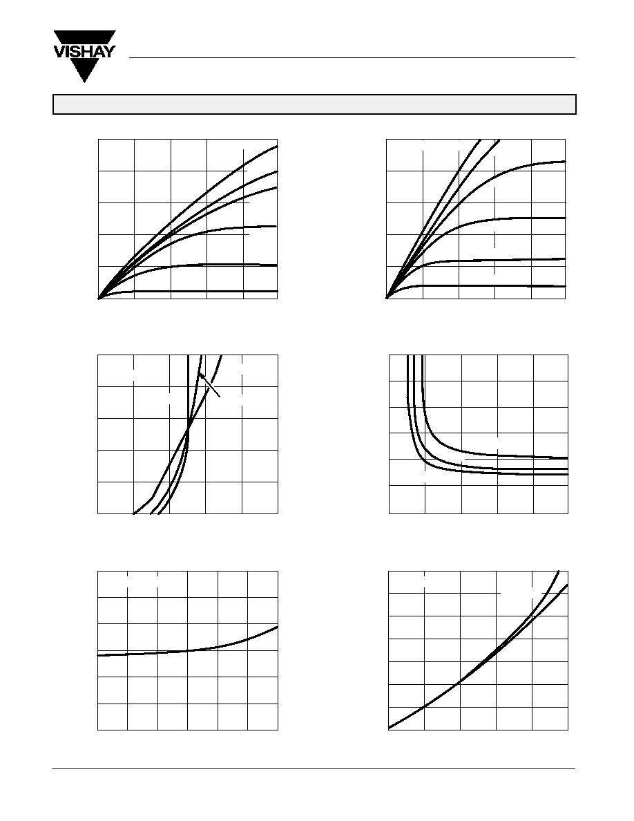
TYPICAL CHARACTERISTICS (T
A
= 25_C UNLESS OTHERWISE NOTED)
Ohmic Region Characteristics
Output Characteristics for Low Gate Drive
V
DS
≠ Drain-to-Source Voltage (V)
V
DS
≠ Drain-to-Source Voltage (V)
1.0
0
1
2
3
4
5
0.8
0.6
0.4
0.2
0
V
GS
= 10 V
4.0 V
3.5 V
3.0 V
2.5 V
2.0 V
200
0
0.4
0.8
1.2
1.6
2.0
160
120
80
40
0
V
GS
= 3 V
2.6 V
2.4 V
2.2 V
2.0 V
1.8 V
On-Resistance vs. Drain Current
Normalized On-Resistance
vs. Junction Temperature
Transfer Characteristics
On-Resistance vs. Gate-to-Source Voltage
V
GS
≠ Gate-Source Voltage (V)
V
GS
≠ Gate-Source Voltage (V)
I
D
≠ Drain Current (A)
T
J
≠ Junction Temperature (
_
C)
0.5
0.4
0.3
0
0
1
5
0.2
0.1
2
3
4
125
_
C
25
_
C
T
J
= ≠55
_
C
6
5
4
0
0
0.1
0.6
3
1
0.2
0.3
0.4
0.5
2
0
4
8
12
16
20
12
10
8
0
6
4
2
I
D
= 0.1 A
0.5 A
1.0 A
2.25
2.00
1.75
0.50
≠50
≠10
150
1.50
1.25
30
70
110
1.00
0.75
0.1 A
V
GS
= 10 V
I
D
= 0.5 A
V
GS
= 10 V
V
DS
= 15 V
I
D
≠
Drain Current (A)
I
D
≠
Drain Current (mA)
I
D
≠
Drain Current (A)
r
DS
(
on)
≠
On-Resistance (
)
r
DS
(
on)
≠
Drain-Source On-Resistance (
)
r
DS
(
on)
≠
Drain-Source On-Resistance (
)
(
Normalized)
TN2410L, VN2406D/L, VN2410L/LS
Vishay Siliconix
www.vishay.com
11-4
Document Number: 70204
S-04279--Rev. F, 16-Jul-01
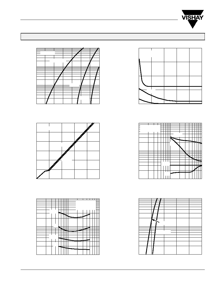
TYPICAL CHARACTERISTICS (T
A
= 25_C UNLESS OTHERWISE NOTED)
Threshold Region
Capacitance
V
DS
≠ Drain-to-Source Voltage (V)
V
GS
≠ Gate-to-Source Voltage (V)
10
1
0.01
0.3
0.1
0.7
1.1
1.5
25
_
C
≠55
_
C
T
J
= 150
_
C
400
300
0
0
10
50
200
100
20
30
40
V
GS
= 0 V
f = 1 MHz
V
DS
= 5 V
C
iss
C
oss
C
rss
100
10
1
1
100
2
10
5
20
50
V
DD
= 60 V
R
L
= 150
W
I
D
= 0.4 A
0.01
0.1
1
100
10
1
V
DS
= 60 V
R
G
= 25
W
Gate Charge
Load Condition Effects on Switching
I
D
≠ Drain Current (A)
Q
g
≠ Total Gate Charge (pC)
t
d(off)
t
d(on)
t
r
t
f
Drive Resistance Effects on Switching
Source-Drain Diode Forward Voltage
t
d(off)
t
d(on)
t
r
t
f
15.0
12.5
10.0
0
0
400
2000
7.5
5.0
800
1200
1600
2.5
192 V
0
0.5
2.5
1
0.1
0.01
1.0
1.5
2.0
T
J
= 25
_
C
T
J
= 150
_
C
V
SD
≠ Source-Drain Voltage (V)
R
G
≠ Gate Resistance (
W
)
I
D
= 0.5 A
V
DS
= 120 V
I
D
≠
Drain Current (mA)
C
≠
Capacitance (pF)
V
GS
≠
Gate-to-Source V
oltage (V)
t
≠
Switching T
ime (ns)
t
≠
Switching T
ime (ns)
I
S
≠
Source Current (A)
TN2410L, VN2406D/L, VN2410L/LS
Vishay Siliconix
Document Number: 70204
S-04279--Rev. F, 16-Jul-01
www.vishay.com
11-5
TYPICAL CHARACTERISTICS (T
A
= 25_C UNLESS OTHERWISE NOTED)
10 K
Duty Cycle = 0.5
0.2
0.1
0.05
0.02
Single Pulse
1
0.01
0.1
0.01
0.1
1
100
10
1 K
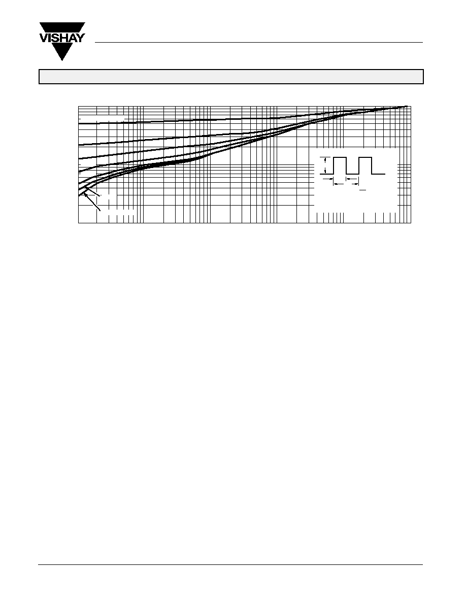
Normalized Effective Transient Thermal Impedance, Junction-to-Ambient (TO-226AA)
Normalized Ef
fective
T
ransient
Thermal Impedance
t
1
≠ Square Wave Pulse Duration (sec)
1. Duty Cycle, D =
2. Per Unit Base = R
thJA
= 156
_
C/W
3. T
JM
≠ T
A
= P
DM
Z
thJA
(t)
t
1
t
2
t
1
Notes:
P
DM
t
2