TP0101T/TS
Vishay Siliconix
Document Number: 70229
S-04279--Rev. D, 16-Jul-01
www.vishay.com
11-1
P-Channel 20-V (D-S) MOSFET, Low-Threshold
PRODUCT SUMMARY
I
D
(A)
V
DS
(V)
r
DS(on)
(
W
)
TP0101T
TP0101TS
0.65 @ V
GS
= ≠4.5 V
≠0.6
≠1.0
≠20
0.85 @ V
GS
= ≠2.5 V
≠0.5
≠0.9
FEATURES
BENEFITS
APPLICATIONS
D
High-Side Switching
D
Low On-Resistance: 0.45
W
D
Low Threshold: 0.9 V (typ)
D
Fast Switching Speed: 32 ns
D
2.5-V or Lower Operation
D
Ease in Driving Switches
D
Low Offset (Error) Voltage
D
Low-Voltage Operation
D
High-Speed Circuits
D
Low Battery Voltage Operation
D
Drivers: Relays, Solenoids, Lamps, Hammers,
Displays, Memories
D
Battery Operated Systems, DC/DC Converters
D
Power Supply Converter Circuits
D
Load/Power Switching≠Cell Phones, Pagers
G
S
D
Top View
2
3
TO-236
(SOT-23)
1
Marking Code:
TP0101T: POwll
TP0101TS: PSwll
w = Week Code
l = Lot Traceability
ABSOLUTE MAXIMUM RATINGS (T
A
= 25_C UNLESS OTHERWISE NOTED)
Parameter
Symbol
TP0101T
TP0101TS
c
Unit
Drain-Source Voltage
V
DS
≠20
≠20
Gate-Source Voltage
V
GS
"
8
"
8
V
_
T
A
= 25
_
C
≠0.6
≠1.0
Continuous Drain Current
(T
J
= 150
_
C)
b
T
A
= 70
_
C
I
D
≠0.48
≠0.8
Pulsed Drain Current
a
I
DM
≠3
≠3
A
Continuous Source Current (Diode Conduction)
b
I
S
≠0.6
≠1.0
T
A
= 25
_
C
0.35
1.0
Power Dissipation
b
T
A
= 70
_
C
P
D
0.22
0.65
W
Operating Junction and Storage Temperature Range
T
J
, T
stg
≠55 to 150
≠55 to 150
_
C
THERMAL RESISTANCE RATINGS
Parameter
Symbol
TP0101T
TP0101TS
c
Unit
Thermal Resistance, Junction-to-Ambient
b
R
thJA
357
125
_
C/W
Notes
a.
Pulse width limited by maximum junction temperature.
b.
Surface Mounted on FR4 Board, t
v
10 sec.
c.
Copper lead frame.
TP0101T/TS
Vishay Siliconix
www.vishay.com
11-2
Document Number: 70229
S-04279--Rev. D, 16-Jul-01
SPECIFICATIONS (T
A
= 25_C UNLESS OTHERWISE NOTED)
Limits
Parameter
Symbol
Test Conditions
Min
Typ
Max
Unit
Static
Drain-Source Breakdown Voltage
V
(BR)DSS
V
GS
= 0 V, I
D
= ≠10
m
A
≠20
≠26
Gate-Threshold Voltage
V
GS(th)
V
DS
= V
GS
, I
D
= ≠50
m
A
≠0.5
≠0.9
≠1.5
V
Gate-Body Leakage
I
GSS
V
DS
= 0 V, V
GS
=
"
8 V
"
100
nA
V
DS
= ≠9.6 V, V
GS
= 0 V
≠1
m
Zero Gate Voltage Drain Current
I
DSS
T
J
= 55
_
C
≠10
m
A
V
DS
v
≠5 V, V
GS
= ≠4.5 V
≠2.5
On-State Drain Current
a
I
D(on)
V
DS
v
≠5 V, V
GS
= ≠2.5 V
≠0.5
A
V
GS
= ≠4.5 V, I
D
= ≠0.6 A
0.45
0.65
W
Drain-Source On-Resistance
a
r
DS(on)
V
GS
= ≠2.5 V, I
D
= ≠0.5 A
0.69
0.85
W
Forward Transconductance
a
g
fs
V
DS
= ≠5 V, I
D
= ≠0.6 A
1300
mS
Diode Forward Voltage
a
V
SD
I
S
= ≠0.6 A, V
GS
= 0 V
≠0.9
≠1.2
V
Dynamic
Total Gate Charge
Q
g
2020
3000
Gate-Source Charge
Q
gs
V
DS
= ≠6 V, V
GS
=≠4.5 V
I
D
^
≠0.6 A
180
pC
Gate-Drain Charge
Q
gd
I
D
^
≠0.6 A
720
Input Capacitance
C
iss
110
Output Capacitance
C
oss
V
DS
= ≠6 V, V
GS
= 0, f = 1 MHz
80
pF
Reverse Transfer Capacitance
C
rss
30
Switching
t
d(on)
7
12
Turn-On Time
t
r
V
DD
= ≠6 V, R
L
= 12
W
^
25
35
t
d(off)
I
D
^
≠0.6 A, V
GEN
= ≠4.5 V
R
G
= 6
W
19
30
ns
Turn-Off Time
t
f
9
15
Notes
a.
Pulse test: PW
v
300
m
s duty cycle
v
2%.
VPLJ01
TP0101T/TS
Vishay Siliconix
Document Number: 70229
S-04279--Rev. D, 16-Jul-01
www.vishay.com
11-3
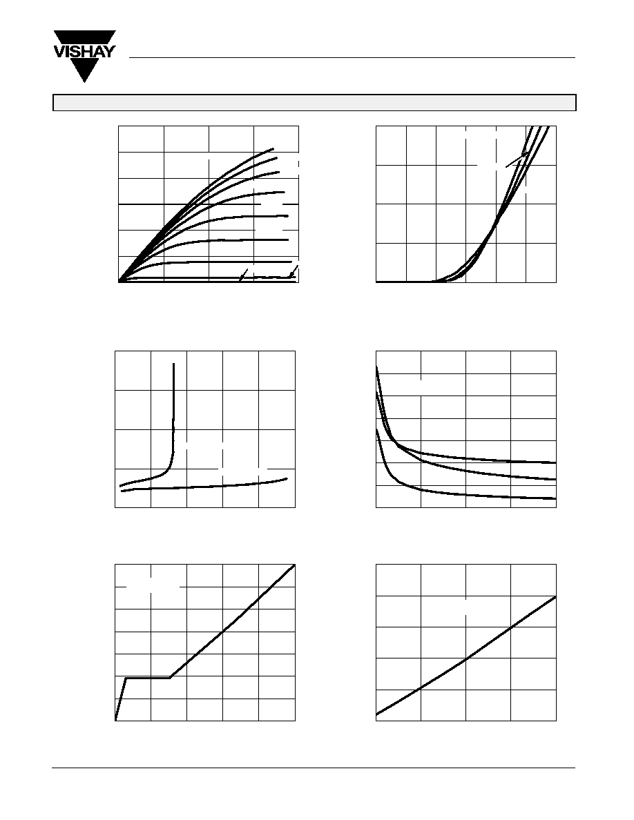
TYPICAL CHARACTERISTICS (T
A
= 25_C UNLESS OTHERWISE NOTED)
≠
≠
≠
≠
On-Resistance vs. Drain Current
Output Characteristics
Transfer Characteristics
V
DS
≠ Drain-to-Source Voltage (V)
V
GS
≠ Gate-to-Source Voltage (V)
0
1
2
3
4
5
6
0
1
2
3
4
0.0
0.5
1.0
1.5
2.0
0.0
0.5
1.0
1.5
2.0
2.5
3.0
25
_
C
T
A
= ≠55
_
C
125
_
C
≠2.5 V
≠3 V
V
GS
= ≠5 V
≠1.5 V
≠2 V
0
50
100
150
200
250
300
350
0
3
6
9
12
0.7
0.9
1.1
1.3
1.5
1.7
≠50
0
50
100
150
0
1
2
3
4
5
6
7
0
600
1200
1800
2400
3000
0
1
2
3
4
0
1
2
3
4
5
Gate Charge
Q
g
≠ Total Gate Charge (pC)
V
DS
≠ Drain-to-Source Voltage (V)
C
oss
C
rss
C
iss
V
DS
= ≠6 V
I
D
= ≠0.5 A
I
D
≠ Drain Current (A)
Capacitance
On-Resistance vs. Junction Temperature
V
GS
= ≠4.5 V
I
D
= ≠0.5 A
T
J
≠ Junction Temperature (
_
C)
V
GS
= ≠2.5 V
V
GS
= ≠4.5 V
≠0.5, 1 V
≠3.5 V
≠4 V
≠4.5 V
I
D
≠
Drain Current (A)
I
D
≠
Drain Current (A)
C
≠
Capacitance (pF)
r
DS
(
on)
≠
Drain-Source On-Resistance (
)
V
GS
≠
Gate-to-Source V
oltage (V)
r
DS
(
on)
≠
On-Resistance (
)
(
Normalized)
≠
≠
≠
≠
≠
≠
≠
≠
≠
≠
≠
≠
≠
≠
≠
≠
≠
≠
≠
≠
≠
≠
≠
≠
≠
≠
V
GS
= 0
f = 1 MHz
≠
≠
≠
≠
≠
≠
≠
≠
≠
≠
TP0101T/TS
Vishay Siliconix
www.vishay.com
11-4
Document Number: 70229
S-04279--Rev. D, 16-Jul-01
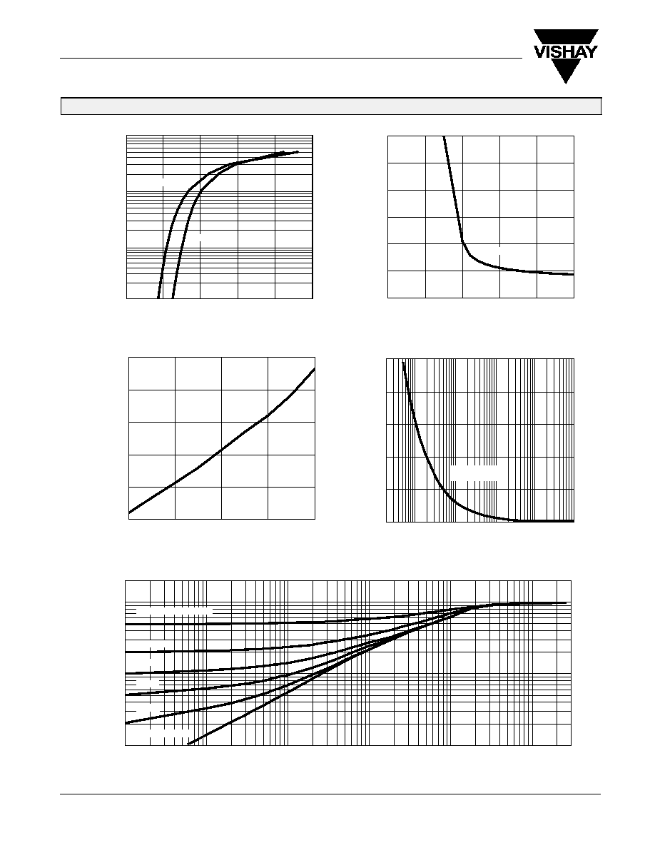
TYPICAL CHARACTERISTICS (T
A
= 25_C UNLESS OTHERWISE NOTED)
0.0
0.5
1.0
1.5
2.0
2.5
≠0.16
≠0.06
0.04
0.14
0.24
0.34
≠50
0
50
100
150
0.0
0.5
1.0
1.5
2.0
2.5
3.0
0
1
2
3
4
5
Source-Drain Diode Forward Voltage
On-Resistance vs. Gate-to-Source Voltage
Threshold Voltage
Single Pulse Power
Normalized Thermal Transient Impedance, Junction-to-Ambient
Square Wave Pulse Duration (sec)
2
1
0.1
0.01
10
≠4
10
≠3
10
≠2
10
≠1
1
Normalized Ef
fective
T
ransient
Thermal Impedance
30
V
SD
≠ Source-to-Drain Voltage (V)
V
GS
≠ Gate-to-Source Voltage (V)
T
J
≠ Junction Temperature (
_
C)
Time (sec)
0.2
0.1
0.05
0.02
Single Pulse
Duty Cycle = 0.5
I
D
= ≠50
m
A
I
D
= ≠0.5 A
10
1
0.1
0.01
0.001
0.01
0.1
1
100
10
10
T
J
= 50
_
C
T
J
= 25
_
C
T
A
= 25
_
C
Single Pulse
8
6
4
2
0
10
I
S
≠
Source Current (A)
r
DS
(
on)
≠
On-Resistance (
)
V
GS
(t
h
)
≠
V
ariance (V)
≠
≠
≠
≠
≠
≠
≠
≠
≠
≠
≠
≠
≠
≠