 | –≠–ª–µ–∫—Ç—Ä–æ–Ω–Ω—ã–π –∫–æ–º–ø–æ–Ω–µ–Ω—Ç: TP0610K | –°–∫–∞—á–∞—Ç—å:  PDF PDF  ZIP ZIP |
TP0610K
Vishay Siliconix
New Product
Document Number: 71411
S-04279--Rev. C, 16-Jul-01
www.vishay.com
11-1
P-Channel 60-V (D-S) MOSFET
PRODUCT SUMMARY
V
(BR)DSS(min)
(V)
r
DS(on)
(
W
)
V
GS(th)
(V)
I
D
(mA)
≠60
6 @ V
GS
= ≠10 V
≠1 to ≠3.0
≠185
FEATURES
BENEFITS
APPLICATIONS
D
High-Side Switching
D
Low On-Resistance: 6
D
Low Threshold: ≠2 V (typ)
D
Fast Swtiching Speed: 20 ns (typ)
D
Low Input Capacitance: 20 pF (typ)
D
Gate-Source ESD Protection
D
Ease in Driving Switches
D
Low Offset (Error) Voltage
D
Low-Voltage Operation
D
High-Speed Circuits
D
Easily Driven Without Buffer
D
Drivers: Relays, Solenoids, Lamps, Hammers,
Displays, Memories, Transistors, etc.
D
Battery Operated Systems
D
Power Supply Converter Circuits
D
Solid State Relays
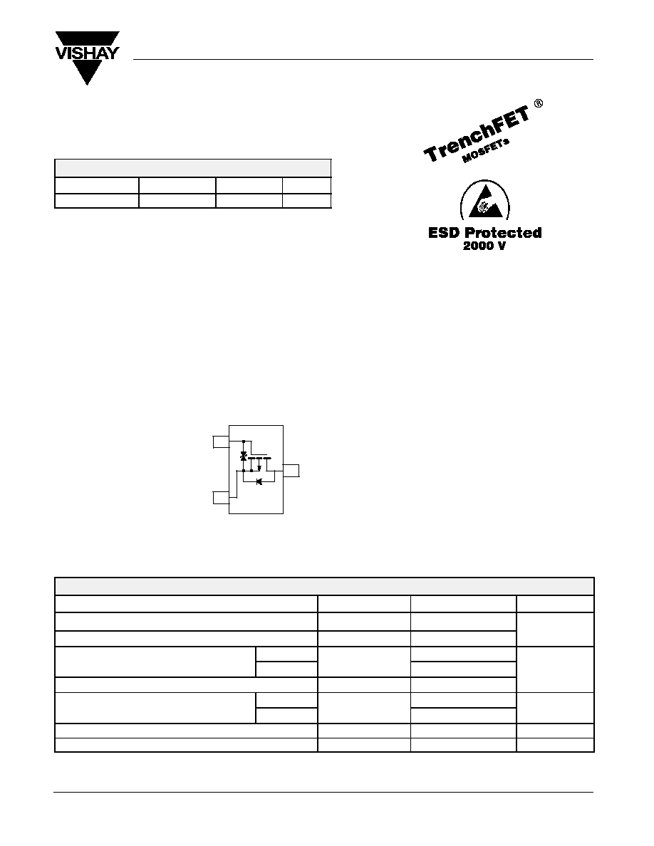
TO-236
(SOT-23)
Top View
2
1
S
D
G
3
Marking Code: 6Kwll
6K = Part Number Code for TP0610K
w = Week Code
ll = Lot Traceability
ABSOLUTE MAXIMUM RATINGS (T
A
= 25_C UNLESS OTHERWISE NOTED)
Parameter
Symbol
Limit
Unit
Drain-Source Voltage
V
DS
≠60
Gate-Source Voltage
V
GS
"
20
V
T
A
= 25
_
C
≠185
Continuous Drain Current
a
T
A
= 100
_
C
I
D
≠115
mA
Pulse Drain Current
b
I
DM
≠800
T
A
= 25
_
C
350
Power Dissipation
a
T
A
= 100
_
C
P
D
140
mW
Maximum Junction-to-Ambient
a
R
thJA
350
_
C/W
Operating Junction and Storage Temperature Range
T
J
, T
stg
≠55 to 150
_
C
Notes
a.
Surface mounted on FR4 board.
b.
Pulse width limited by maximum junction temperature.

TP0610K
Vishay Siliconix
New Product
www.vishay.com
11-2
Document Number: 71411
S-04279--Rev. C, 16-Jul-01
SPECIFICATIONS (T
A
= 25_C UNLESS OTHERWISE NOTED)
Parameter
Symbol
Test Condition
Min
Typ
Max
Unit
Static
Drain-Source Breakdown Voltage
V
(BR)DSS
V
GS
= 0 V, I
D
= ≠10
µ
A
≠60
Gate-Threshold Voltage
V
GS(th)
V
DS
= V
GS
, I
D
= ≠250
µ
A
≠1
≠3.0
V
V
DS
= 0 V, V
GS
=
"
20 V
"
10
m
A
V
DS
= 0 V, V
GS
=
"
10 V
"
200
Gate-Body Leakage
I
GSS
V
DS
= 0 V, V
GS
=
"
10 V, T
J
= 85
_
C
"
500
V
DS
= 0 V, V
GS
=
"
5 V
"
100
nA
V
DS
= ≠50 V, V
GS
= 0 V
≠25
Zero Gate Voltage Drain Current
I
DSS
V
DS
= ≠50 V, V
GS
= 0 V, T
J
= 85
_
C
≠250
V
DS
= ≠10 V, V
GS
= ≠4.5 V
≠50
On-State Drain Current
a
I
D(on)
V
DS
= ≠10 V, V
GS
= ≠10 V
≠600
mA
V
GS
= ≠4.5 V, I
D
= ≠25 mA
10
Drain-Source On-Resistance
a
r
DS(on)
V
GS
= ≠10 V, I
D
= ≠500 mA
6
W
DS(on)
V
GS
= ≠10 V, I
D
= ≠500 mA, T
J
= 125
_
C
9
Forward Transconductance
a
g
fs
V
DS
= ≠10 V, I
D
= ≠100 mA
80
mS
Diode Forward Voltage
a
V
SD
I
S
= ≠200 mA, V
GS
= 0 V
≠1.4
V
Dynamic
Total Gate Charge
Q
g
1.7
Gate-Source Charge
Q
gs
V
DS
= ≠30 V, V
GS
= ≠15 V, I
D
^
≠500 mA
0.26
nC
Gate-Drain Charge
Q
gd
DS
GS
D
0.46
Input Capacitance
C
iss
23
Output Capacitance
C
oss
V
DS
= ≠25 V, V
GS
= 0 V, f = 1 MHz
10
pF
Reverse Transfer Capacitance
C
rss
DS
GS
5
Switching
b
Turn-On Time
t
ON
V
DD
= ≠25 V, R
L
= 150
W
^
20
Turn-Off Time
t
OFF
I
D
^
≠200 mA, V
GEN
= ≠10 V
R
G
= 10
W
35
ns
Notes
a.
Pulse test: PW
v
300 ms duty cycle
v
2%.
TPJO60
b.
Switching time is essentially independent of operating temperature.

TP0610K
Vishay Siliconix
New Product
Document Number: 71411
S-04279--Rev. C, 16-Jul-01
www.vishay.com
11-3
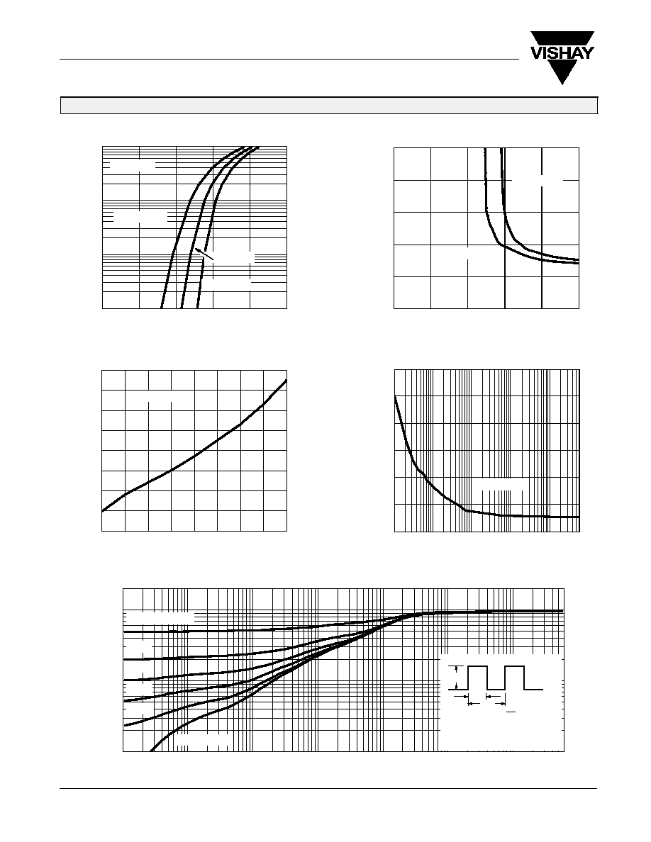
TYPICAL CHARACTERISTICS (25_C UNLESS NOTED)
0
300
600
900
1200
0
2
4
6
8
10
0.0
0.2
0.4
0.6
0.8
1.0
0
1
2
3
4
5
Output Characteristics
Transfer Characteristics
V
DS
≠ Drain-to-Source Voltage (V)
≠
Drain Current (A)
I
D
V
GS
= 10 V
5 V
4 V
V
GS
≠ Gate-to-Source Voltage (V)
≠
Drain Current (mA)
I
D
T
J
= ≠55
_
C
125
_
C
25
_
C
0.0
0.3
0.6
0.9
1.2
1.5
1.8
≠50
≠25
0
25
50
75
100
125
150
On-Resistance vs. Junction Temperature
T
J
≠ Junction Temperature (
_
C)
V
GS
= 10 V @ 500 mA
V
GS
= 4.5 V @ 25 mA
(Normalized)
≠
On-Resistance (
r DS(on)
W
)
0
3
6
9
12
15
0.0
0.3
0.6
0.9
1.2
1.5
1.8
I
D
= 500 mA
Gate Charge
≠
Gate-to-Source V
oltage (V)
Q
g
≠ Total Gate Charge (nC)
V
GS
0
4
8
12
16
20
0
200
400
600
800
1000
On-Resistance vs. Drain Current
I
D
≠ Drain Current (mA)
V
GS
= 4.5 V
V
GS
= 10 V
≠
On-Resistance (
r DS(on)
W
)
0
8
16
24
32
40
0
5
10
15
20
25
Capacitance
V
DS
≠ Drain-to-Source Voltage (V)
C
≠
Capacitance (pF)
C
rss
C
oss
C
iss
V
GS
= 0 V
6 V
7 V
V
GS
= 5 V
V
DS
= 30 V
V
DS
= 48 V
8 V
For the following graphs, p-channel negative polarities for all voltage and current values are represented as positive values.
TP0610K
Vishay Siliconix
New Product
www.vishay.com
11-4
Document Number: 71411
S-04279--Rev. C, 16-Jul-01
TYPICAL CHARACTERISTICS (25_C UNLESS NOTED)
0
2
4
6
8
10
0
2
4
6
8
10
On-Resistance vs. Gate-Source Voltage
V
GS
≠ Gate-to-Source Voltage (V)
I
D
= 500 mA
I
D
= 200 mA
≠
On-Resistance (
r DS(on)
W
)
1.2
1.5
1
100
1000
0.00
0.3
0.6
0.9
T
J
= 25
_
C
T
J
= 125
_
C
Source-Drain Diode Forward Voltage
V
SD
≠ Source-to-Drain Voltage (V)
≠
Source Current (A)
I
S
10
T
J
= ≠55
_
C
V
GS
= 0 V
Threshold Voltage Variance Over Temperature
V
ariance (V)
V
GS(th)
≠0.3
≠0.2
≠0.1
≠0.0
0.1
0.2
0.3
0.4
0.5
≠50
≠25
0
25
50
75
100
125
150
I
D
= 250
m
A
T
J
≠ Junction Temperature (
_
C)
10
≠3
10
≠2
1
10
600
10
≠1
10
≠4
100
2
1
0.1
0.01
0.2
0.1
0.05
0.02
Single Pulse
Duty Cycle = 0.5
Normalized Thermal Transient Impedance, Junction-to-Ambient
Square Wave Pulse Duration (sec)
Normalized Ef
fective
T
ransient
Thermal Impedance
1. Duty Cycle, D =
2. Per Unit Base = R
thJA
= 350
_
C/W
3. T
JM
≠ T
A
= P
DM
Z
thJA
(t)
t
1
t
2
t
1
t
2
Notes:
4. Surface Mounted
P
DM
0.01
0
1
2.5
3
100
600
0.1
Power (W)
Single Pulse Power, Junction-to-Ambient
Time (sec)
1.5
2
0.5
1
10
T
A
= 25
_
C
For the following graphs, p-channel negative polarities for all voltage and current values are represented as positive values.