 | –≠–ª–µ–∫—Ç—Ä–æ–Ω–Ω—ã–π –∫–æ–º–ø–æ–Ω–µ–Ω—Ç: TSMG3700 | –°–∫–∞—á–∞—Ç—å:  PDF PDF  ZIP ZIP |
VISHAY
TSMG3700
Document Number 81081
Rev. 1.4, 22-Jun-04
Vishay Semiconductors
www.vishay.com
1
94 8553
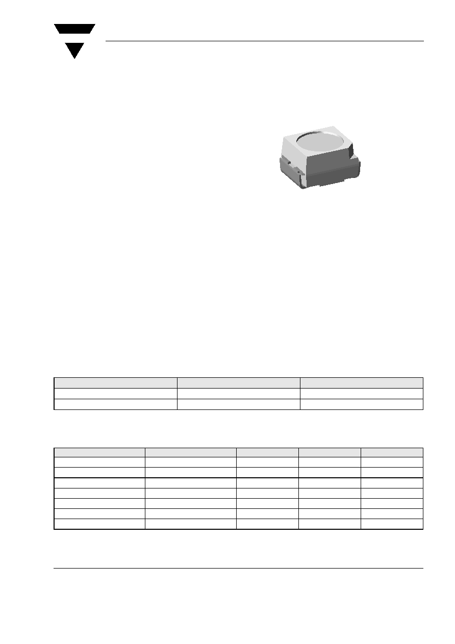
GaAlAs DH Infrared Emitting Diode in SMT Package
Description
TSMG3700 is a high speed infrared emitting diode in
GaAlAs double hetero (DH) technology in a miniature
PLCC-2 SMD package.
DH technology combines high speed with high radiant
power at wavelength of 850 nm.
Features
∑ High radiant power
∑ High speed
∑ High modulation band width
∑ Peak wavelength
p
= 850 nm
∑ High reliability
∑ Low forward voltage
∑ Suitable for high pulse current application
∑ Wide angle of half intensity
∑ Compatible with automatic placement equipment
∑ EIA and ICE standard package
∑ Suitable for infrared, vapor phase and
wavesolder process
∑ 8 mm tape and reel standard: GS08
∑ Lead free component
Applications
Infrared source for CMOS cameras
High speed IR data transmission
Parts Table
Absolute Maximum Ratings
T
amb
= 25 ∞C, unless otherwise specified
Part
Ordering code
Remarks
TSMG3700
TSMG3700-GS08
MOQ: 7500 pcs
TSMG3700
TSMG3700-GS18
MOQ: 8000 pcs
Parameter
Test condition
Symbol
Value
Unit
Reverse Voltage
V
R
5
V
Forward current
I
F
100
mA
Peak Forward Current
t
p
/T = 0.5, t
p
= 100
µs
I
FM
200
mA
Surge Forward Current
t
p
= 100
µs
I
FSM
1
A
Power Dissipation
P
V
170
mW
Junction Temperature
T
j
100
∞C
Operating Temperature Range
T
amb
- 40 to + 85
∞C
www.vishay.com
2
Document Number 81081
Rev. 1.4, 22-Jun-04
VISHAY
TSMG3700
Vishay Semiconductors
Basic Characteristics
T
amb
= 25 ∞C, unless otherwise specified
Typical Characteristics
(T
amb
= 25
∞C unless otherwise specified)
Storage Temperature Range
T
stg
- 40 to + 100
∞C
Soldering Temperature
t
10 sec
T
sd
260
∞C
Thermal Resistance Junction/
Ambient
R
thJA
450
K/W
Parameter
Test condition
Symbol
Min
Typ.
Max
Unit
Forward Voltage
I
F
= 100 mA, t
p
= 20 ms
V
F
1.5
1.8
V
I
F
= 1 A, t
p
= 100
µs
V
F
2.3
V
Temp. Coefficient of V
F
I
F
= 100 mA
TK
VF
-2.1
mV/K
Reverse Current
V
R
= 5 V
I
R
10
µA
Junction capacitance
V
R
= 0 V, f = 1 MHz, E = 0
C
j
125
pF
Radiant Intensity
I
F
= 100 mA, t
p
= 20 ms
I
e
6
10
22
mW/sr
I
F
= 1 A, t
p
= 100
µs
I
e
100
mW/sr
Radiant Power
I
F
= 100 mA, t
p
= 20 ms
e
40
mW
Temp. Coefficient of
e
I
F
= 100 mA
TK
e
-0.35
%/K
Angle of Half Intensity
± 60
deg
Peak Wavelength
I
F
= 100 mA
p
850
nm
Spectral Bandwidth
I
F
= 100 mA
40
nm
Temp. Coefficient of
p
I
F
= 100 mA
TK
p
0.25
nm/K
Rise Time
I
F
= 100 mA
t
r
20
ns
Fall Time
I
F
= 100 mA
t
f
13
ns
Virtual Source Diameter
0.44
mm
Parameter
Test condition
Symbol
Value
Unit
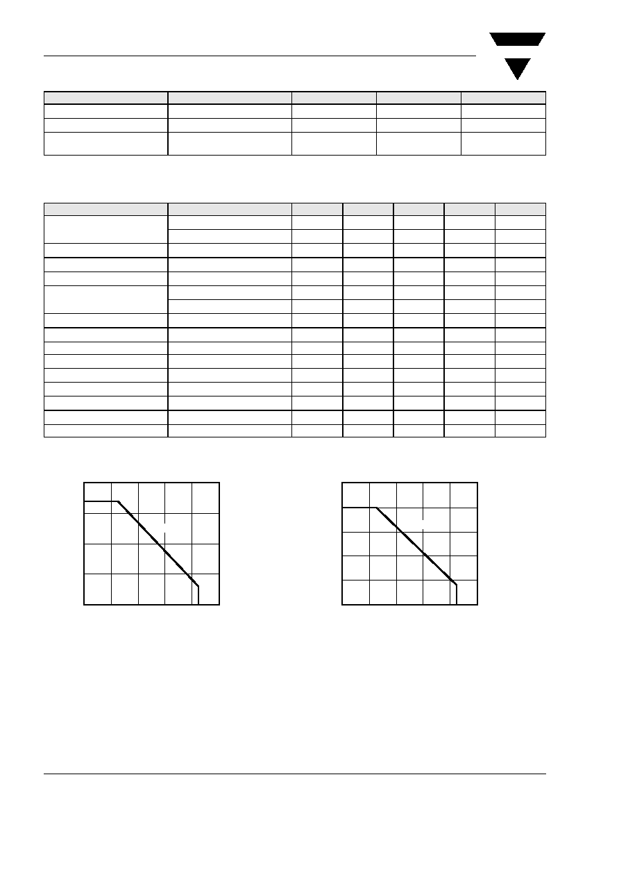
Figure 1. Power Dissipation vs. Ambient Temperature
0
50
100
150
200
14846
P
-
Power
Dissipation
(
m
W
)
V
R
thJA
T
amb
- Ambient Temperature (∞C )
0
20
40
60
80
100
Figure 2. Forward Current vs. Ambient Temperature
0
25
50
75
100
125
14847
R
thJA
I
-
Forward
Current
(
m
A
)
F
T
amb
- Ambient Temperature ( ∞C )
0
20
40
60
80
100
VISHAY
TSMG3700
Document Number 81081
Rev. 1.4, 22-Jun-04
Vishay Semiconductors
www.vishay.com
3
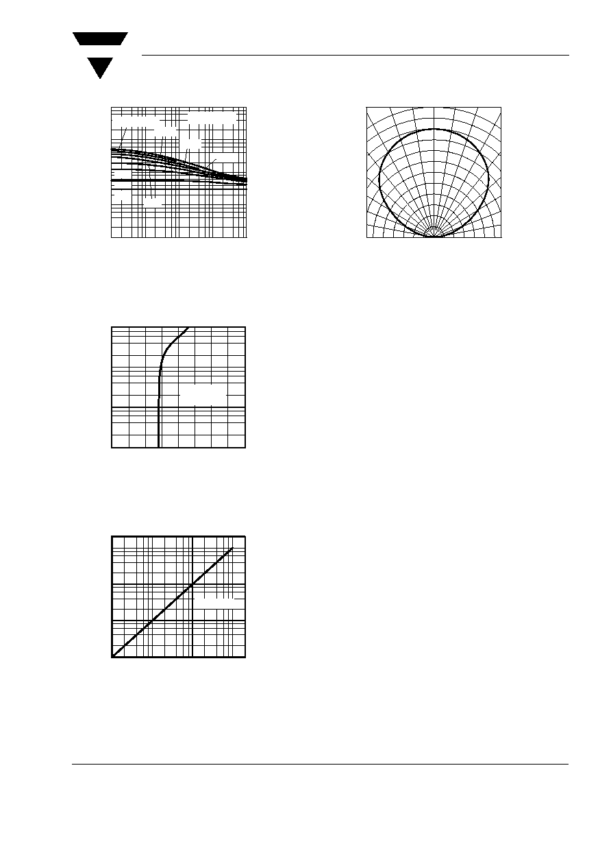
Figure 3. Pulse Forward Current vs. Pulse Duration
Figure 4. Forward Current vs. Forward Voltage
Figure 5. Radiant Intensity vs. Forward Pulse Current
0.01
0.1
1
10
1
10
100
1000
10000
t
p
- Pulse Length ( ms )
100
95 9985
I
-
Forward
Current
(
m
A
)
F
DC
t
p
/T = 0.005
0.5
0.2
0.1
0.01
0.05
0.02
T
amb
< 60
∞C
18873
F
I
-
Forward
Current
(
m
A
)
1000
100
10
1
V
F
- Forward Voltage ( V )
0
1
2
3
4
t = 100
µs
p
t / T = 0.001
p
0.1
1
10
100
1
10
100
1000
18874
I
F
- Forward Pulse Current ( mA )
I
-
Radiant
Intensity
(
mW/sr
)
e
t = 100 µs
p
Figure 6. Relative Radiant Intensity vs. Angular Displacement
0.4
0.2
0
0.2
0.4
I
-
Relative
Radiant
Intensity
e
rel
0.6
94 8013
0.6
0.9
0.8
0∞
30∞
10∞
20∞
40∞
50∞
60∞
70∞
80∞
0.7
1.0
www.vishay.com
4
Document Number 81081
Rev. 1.4, 22-Jun-04
VISHAY
TSMG3700
Vishay Semiconductors
Package Dimensions in mm
95 11314
Mounting Pad Layout
3.5 ± 0.2
0.85
1.65
+
0.10
-
0.05
Pin identification
2.8
+
0.15
2.2
2.4
3
+ 0.15
1.2
2.6
(2.8)
1.6 (1.9)
4
4
area covered with
solder resist
Dimensions: IR and Vaporphase
(Wave Soldering)
technical drawings
according to DIN
specifications
Drawing-No. : 6.541-5025.01-4
Issue: 7; 05.04.04
C
A
VISHAY
TSMG3700
Document Number 81081
Rev. 1.4, 22-Jun-04
Vishay Semiconductors
www.vishay.com
5
Temperature - Time Profile
Drypack
Devices are packed in moisture barrier bags (MBB) to
prevent the products from moisture absorption during
transportation and storage. Each bag contains a des-
iccant.
Floor Life
Floor life (time between soldering and removing from
MBB) must not exceed the time indicated in
J-STD-020. TSM... is released for:
Moisture Sensitivity Level 2, according to
JEDEC, J-STD-020
Floor Life: 1 year
Conditions: T
amb
< 30 ∞C, RH < 60 %
Drying
In case of moisture absorption devices should be
baked before soldering. Conditions see J-STD-020 or
Label. Devices taped on reel dry using recommended
conditions 192 h @ 40 ∞C (+ 5 ∞C), RH < 5 %
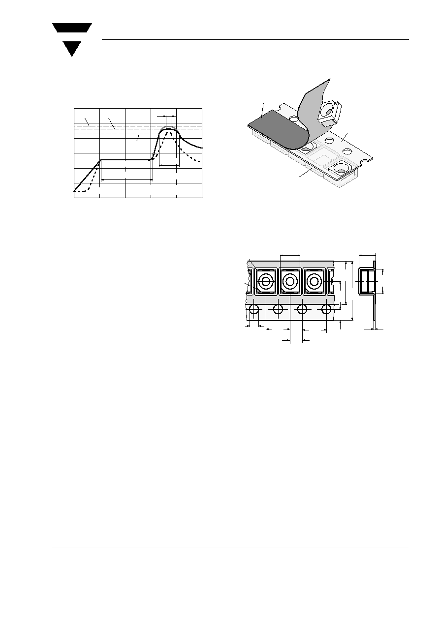
Figure 7. Infrared Reflow Soldering Optodevices (SMD Package)
max. 160 C
full line
: typical
dotted line : process limits
Time ( s )
T
e
mperature
(
C
)
Lead Temperature
90 s - 120 s
300
250
200
150
100
50
0
0
50
100
150
200
250
max. 240 C ca. 230 C
10 s
215 C
max 40 s
2 K/s - 4 K/s
94 8625
∞
∞
∞
∞
∞
Figure 8. Blister Tape
Figure 9. Tape Dimensions in mm for PLCC-2
Adhesive Tape
Component Cavity
Blister Tape
94 8670
1.85
1.65
4.0
3.6
3.6
3.4
2.05
1.95
1.6
1.4
4.1
3.9
4.1
3.9
5.75
5.25
8.3
7.7
3.5
3.1
2.2
2.0
0.25
94 8668
Anode
Cathode