 | –≠–ª–µ–∫—Ç—Ä–æ–Ω–Ω—ã–π –∫–æ–º–ø–æ–Ω–µ–Ω—Ç: TSOP17 | –°–∫–∞—á–∞—Ç—å:  PDF PDF  ZIP ZIP |
VISHAY
TSOP17..KA1
Document Number 82033
Rev. 10, 15-Oct-2002
Vishay Semiconductors
www.vishay.com
1
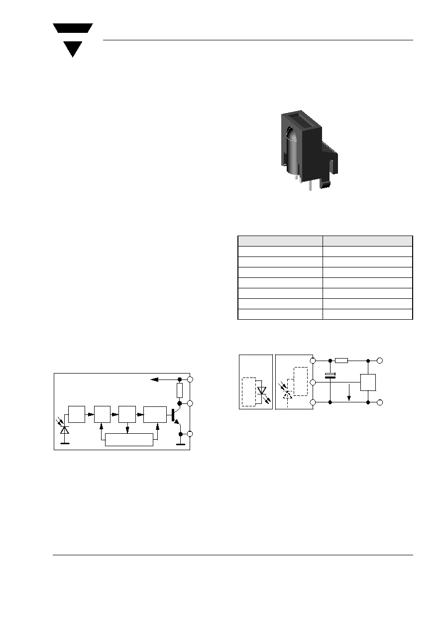
12797
IR Receiver Modules for Remote Control Systems
Description
The TSOP17..KA1 - series are miniaturized receivers
for infrared remote control systems. PIN diode and
preamplifier are assembled on lead frame, the epoxy
package is designed as IR filter.
The demodulated output signal can directly be
decoded by a microprocessor. TSOP17..KA1 is the
standard IR remote control receiver series, support-
ing all major transmission codes.
Features
∑ Photo detector and preamplifier in one package
∑ Internal filter for PCM frequency
∑ Improved shielding against electrical field distur-
bance
∑ TTL and CMOS compatibility
∑ Output active low
∑ Low power consumption
Special Features
∑ Continuous data transmission possible (up to
2400 bps)
∑ Suitable burst length
10 cycles/burst
Block Diagram
Parts Table
Application Circuit
25 k
2
3
1
V
S
OUT
Demo-
GND
Pass
AGC
Input
PIN
Band
dulator
Control Circuit
Part
Carrier Frequency
TSOP1730KA1
30 kHz
TSOP1733KA1
33 kHz
TSOP1736KA1
36 kHz
TSOP1737KA1
36.7 kHz
TSOP1738KA1
38 kHz
TSOP1740KA1
40 kHz
TSOP1756KA1
56 kHz
C
1
=
4.7 µF
TSOPxxxx
OUT
GND
Circuit
µC
R
1
= 100
+V
S
GND
Transmitter
with
TSALxxxx
V
S
R
1
+ C
1
recommended to suppress power supply
disturbances.
V
O
The output voltage should not be hold continuously at
a voltage below V
O =
3.3 V by the external circuit.
Document Number 82033
Rev. 10, 15-Oct-2002
www.vishay.com
2
VISHAY
TSOP17..KA1
Vishay Semiconductors
Absolute Maximum Ratings
T
amb
= 25 ∞C, unless otherwise specified
Electrical and Optical Characteristics
T
amb
= 25 ∞C, unless otherwise specified
Typical Characteristics
(T
amb
= 25∞C unless otherwise specified)
Parameter
Test condition
Symbol
Value
Unit
Supply Voltage
(Pin 2)
V
S
- 0.3 to +
6.0
V
Supply Current
(Pin 2)
I
S
5
mA
Output Voltage
(Pin 3)
V
O
- 0.3 to +
6.0
V
Output Current
(Pin 3)
I
O
5
mA
Junction Temperature
T
j
100
∞C
Storage Temperature Range
T
stg
- 25 to + 85
∞C
Operating Temperature Range
T
amb
- 25 to + 85
∞C
Power Consumption
(T
amb
85 ∞C)
P
tot
50
mW
Soldering Temperature
t
5 s
T
sd
260
∞C
Parameter
Test condition
Symbol
Min
Typ.
Max
Unit
Supply Current (Pin 2)
V
S
= 5 V, E
v
= 0
I
SD
0.8
1.2
1.5
mA
V
S
= 5 V, E
v
= 40 klx, sunlight
I
SH
1.5
mA
Supply Voltage (Pin 2)
V
S
4.5
5.5
V
Transmission Distance
E
v
= 0, test signal see fig.1, IR
diode TSAL6200, I
F
= 400 mA
d
35
m
Output Voltage Low (Pin 3)
I
OSL
= 0.5 mA, E
e
= 0.7 mW/m
2
, f
= f
o
, test signal see fig. 1
V
OSL
250
mV
Irradiance (30 - 40 kHz)
Pulse width tolerance: t
pi
- 5/f
o
< t
po
< t
pi
+ 6/f
o
, test signal see fig.1
E
e min
0.35
0.5
mW/m
2
Irradiance (56 kHz)
Pulse width tolerance: t
pi
- 5/f
o
< t
po
< t
pi
+ 6/f
o
, test signal see fig.1
E
e min
0.4
0.6
mW/m
2
Irradiance
t
pi
- 5/f
o
< t
po
< t
pi
+ 6/f
o
, test signal
see fig. 1
E
e max
30
W/m
2
Directivity
Angle of half transmission distance
1/2
± 45
deg
Figure 1. Output Function
E
e
T
t
pi
*
t
* t
pi
w 10/fo is recommended for optimal function
V
O
V
OH
V
OL
t
16110
Optical Test Signal
(IR diode TSAL6200, I
F
= 0.4 A, 30 pulses, f = f
0
, T = 10 ms)
Output Signal
t
d
1 )
t
po
2 )
1 )
7/f
0
< t
d
< 15/f
0
2 )
t
pi
≠5/f
0
< t
po
< t
pi
+6/f
0
Figure 2. Pulse Length and Sensitivity in Dark Ambient
0.0
0.1
0.2
0.3
0.4
0.5
0.6
0.7
0.8
0.9
1.0
0.1
1.0
10.0
100.0 1000.010000.0
E
e
≠ Irradiance ( mW/m
2
)
16908
Input Burst Duration
l = 950 nm,
optical test signal, fig.1
Output Pulse
t ≠ Output Pulse Width ( ms )
po
VISHAY
TSOP17..KA1
Document Number 82033
Rev. 10, 15-Oct-2002
Vishay Semiconductors
www.vishay.com
3
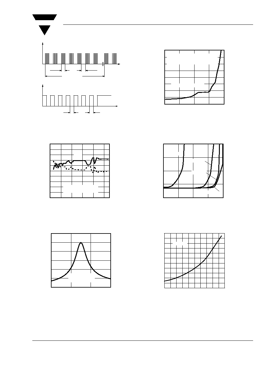
Figure 3. Output Function
Figure 4. Output Pulse Diagram
Figure 5. Frequency Dependence of Responsivity
E
e
t
V
O
V
OH
V
OL
t
600
ms
600
ms
T = 60 ms
T
on
T
off
94 8134
Optical Test Signal
Output Signal, ( see Fig.4 )
T
,T
≠ Output Pulse Width ( ms )
0.0
0.1
0.2
0.3
0.4
0.5
0.6
0.7
0.8
0.9
1.0
0.1
1.0
10.0
100.0 1000.010000.0
E
e
≠ Irradiance ( mW/m
2
)
16909
Toff
l = 950 nm,
optical test signal, fig.3
Ton
on
off
0.0
0.2
0.4
0.6
0.8
1.0
1.2
0.7
0.9
1.1
1.3
f/f
0
≠ Relative Frequency
16925
f = f
0
"5%
Df ( 3dB ) = f
0
/10
E / E ≠ Rel. Responsivity
e min
e
Figure 6. Sensitivity in Bright Ambient
Figure 7. Sensitivity vs. Supply Voltage Disturbances
Figure 8. Sensitivity vs. Electric Field Disturbances
0.0
0.5
1.0
1.5
2.0
2.5
3.0
3.5
4.0
0.01
0.10
1.00
10.00
100.00
E ≠ Ambient DC Irradiance (W/m
2
)
16911
Correlation with ambient light sources:
10W/m
2
^1.4klx (Std.illum.A,T=2855K)
10W/m
2
^8.2klx (Daylight,T=5900K)
Ambient,
l = 950 nm
E ≠
Threshold Irradiance ( mW/m )
e min
2
0.0
0.5
1.0
1.5
2.0
0.1
1.0
10.0
100.0
1000.0
DV
sRMS
≠ AC Voltage on DC Supply Voltage (mV)
16912
f = f
o
f = 10 kHz
E ≠
Threshold Irradiance ( mW/m )
e min
2
f = 1 kHz
f = 100 Hz
E ≠
Threshold Irradiance ( mW/m )
0.0
0.4
0.8
1.2
1.6
0.0
0.4
0.8
1.2
2.0
E ≠ Field Strength of Disturbance ( kV/m )
2.0
94 8147
1.6
e min
2
f(E) = f
0
Document Number 82033
Rev. 10, 15-Oct-2002
www.vishay.com
4
VISHAY
TSOP17..KA1
Vishay Semiconductors
Suitable Data Format
The circuit of the TSOP17..KA1 is designed in that
way that unexpected output pulses due to noise or
disturbance signals are avoided. A bandpassfilter, an
integrator stage and an automatic gain control are
used to suppress such disturbances.
The distinguishing mark between data signal and dis-
turbance signal are carrier frequency, burst length
and duty cycle.
The data signal should fulfill the following conditions:
∑ Carrier frequency should be close to center fre-
quency of the bandpass (e.g. 38 kHz).
∑ Burst length should be 10 cycles/burst or longer.
∑ After each burst which is between 10 cycles and 70
cycles a gap time of at least 14 cycles is necessary.
∑ For each burst which is longer than 1.8 ms a corre-
sponding gap time is necessary at some time in the
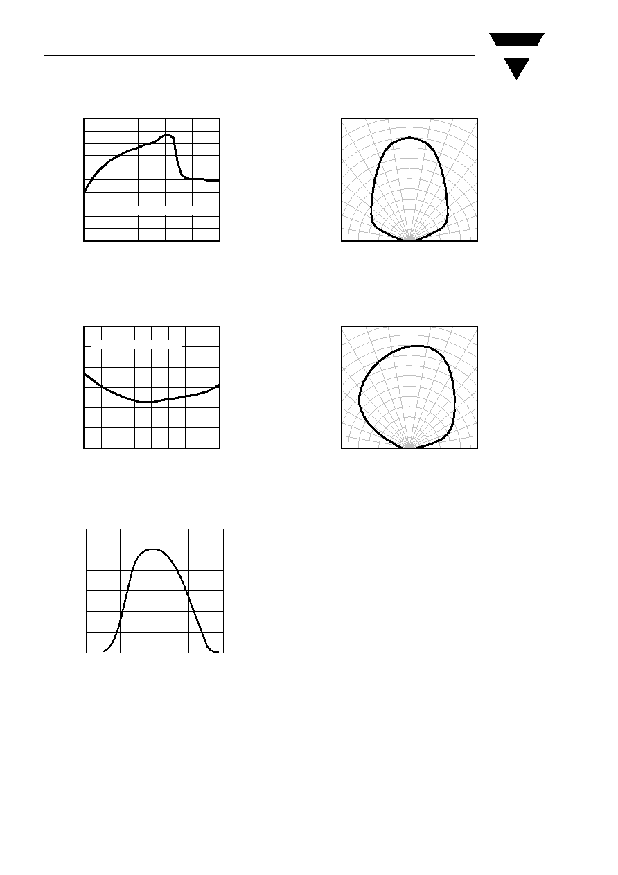
Figure 9. Max. Envelope Duty Cycle vs. Burstlength
Figure 10. Sensitivity vs. Ambient Temperature
Figure 11. Relative Spectral Sensitivity vs. Wavelength
0.0
0.1
0.2
0.3
0.4
0.5
0.6
0.7
0.8
0.9
1.0
10
30
50
70
90
110
Burst Length ( number of cycles / burst )
16915
f = 38 kHz, E
e
= 2 mW/m
2
Max. Envelope Duty Cycle
0.0
0.1
0.2
0.3
0.4
0.5
0.6
≠30 ≠15
0
15
30
45
60
75
90
T
amb
≠ Ambient Temperature ( C )
16918
Sensitivity in dark ambient
E ≠
Threshold Irradiance ( mW/m )
e min
2
750
850
950
1050
0
0.2
0.4
0.6
0.8
1.2
S ( ) ≠ Relative Spectral Sensitivity
rel
l ≠ Wavelength ( nm )
1150
94 8408
1.0
l
Figure 12. Horizontal Directivity
x
Figure 13. Vertical Directivity
y
95 11340p2
0.4
0.2
0
0.2
0.4
0.6
0.6
0.9
0
30
10
20
40
50
60
70
80
1.0
0.8
0.7
d
rel
≠ Relative Transmission Distance
95 11339p2
0.4
0.2
0
0.2
0.4
0.6
0.6
0.9
0
30
10
20
40
50
60
70
80
1.0
0.8
0.7
d
rel
≠ Relative Transmission Distance
VISHAY
TSOP17..KA1
Document Number 82033
Rev. 10, 15-Oct-2002
Vishay Semiconductors
www.vishay.com
5
data stream. This gap time should have at least same
length as the burst.
∑ Up to 1400 short bursts per second can be received
continuously.
Some examples for suitable data format are: NEC
Code, Toshiba Micom Format, Sharp Code, RC5
Code, RC6 Code, R-2000 Code, Sony Format
(SIRCS).
When a disturbance signal is applied to the
TSOP17..KA1 it can still receive the data signal. How-
ever the sensitivity is reduced to that level that no
unexpected pulses will occure.
Some examples for such disturbance signals which
are suppressed by the TSOP17..KA1 are:
∑ DC light (e.g. from tungsten bulb or sunlight)
∑ Continuous signal at 38 kHz or at any other fre-
quency
∑ Signals from fluorescent lamps with electronic bal-
last (an example of the signal modulation is in the fig-
ure below).
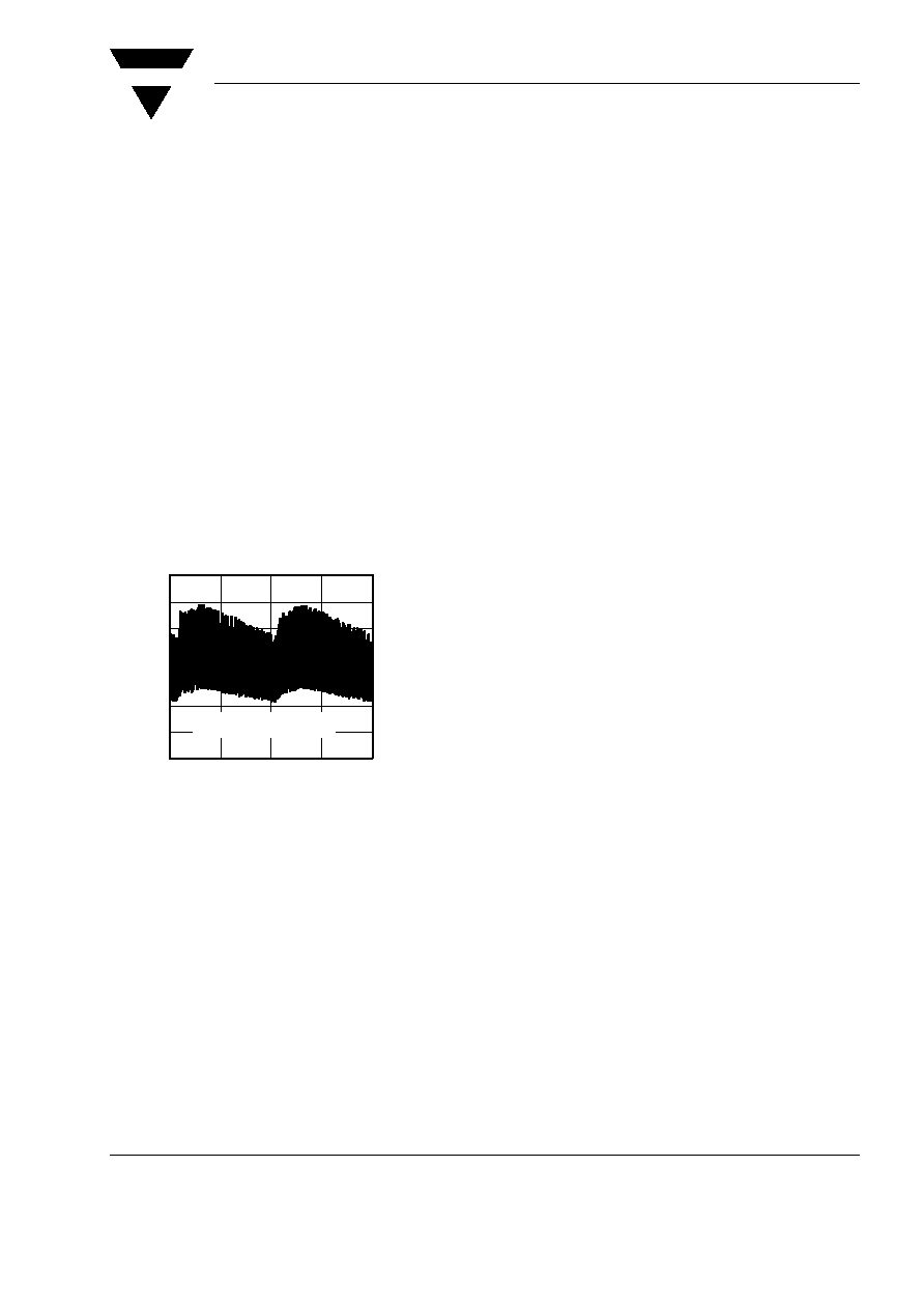
Figure 14. IR Signal from Fluorescent Lamp with low Modulation
0
5
10
15
20
Time ( ms )
16920
IR Signal
IR Signal from fluorescent
lamp with low modulation