Äîêóìåíòàöèÿ è îïèñàíèÿ www.docs.chipfind.ru
TSOP21..YA1
Vishay Telefunken
1 (8)
Rev. 5, 30-Mar-01
www.vishay.com
Document Number 82117
Photo Modules for PCM Remote Control Systems
Available types for different carrier frequencies
Type
fo
Type
fo
TSOP2130YA1
30 kHz
TSOP2133YA1
33 kHz
TSOP2136YA1
36 kHz
TSOP2137YA1
36.7 kHz
TSOP2138YA1
38 kHz
TSOP2140YA1
40 kHz
TSOP2156YA1
56 kHz
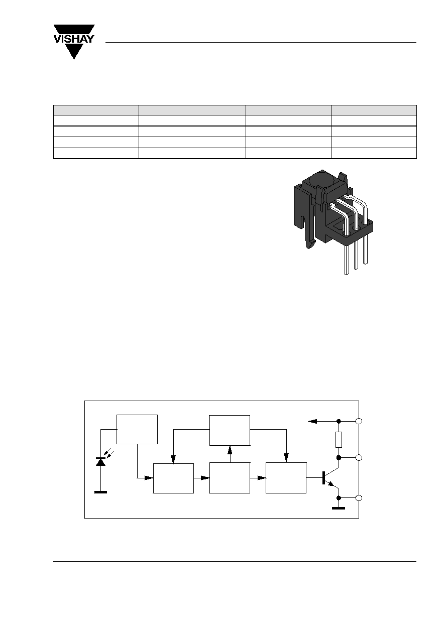
Description
The TSOP21..YA1 series are miniaturized receivers
for infrared remote control systems. PIN diode and
preamplifier are assembled on lead frame, the epoxy
package is designed as IR filter.
The demodulated output signal can directly be
decoded by a microprocessor. The main benefit is the
reliable function even in disturbed ambient and the
protection against uncontrolled output pulses.
16 083
Features
D
Photo detector and preamplifier in one package
D
Internal filter for PCM frequency
D
Improved shielding against electrical field
disturbance
D
TTL and CMOS compatibility
D
Output active low
D
Low power consumption
D
High immunity against ambient light
D
Enhanced data rate of 2400 bit/s
D
Operation with short bursts possible
(
6 cycles/burst)
Block Diagram
14318
PIN
Input
AGC
Control
Circuit
Band
Pass
Demodu-
lator
30 k
W
3
2
1
V
S
OUT
GND
TSOP21..YA1
Vishay Telefunken
Rev. 5, 30-Mar-01
www.vishay.com
Document Number 82117
2 (8)
Absolute Maximum Ratings
T
amb
= 25
_
C
Parameter
Test Conditions
Symbol
Value
Unit
Supply Voltage
(Pin 2)
V
S
0.3...6.0
V
Supply Current
(Pin 2)
I
S
5
mA
Output Voltage
(Pin 1)
V
O
0.3...6.0
V
Output Current
(Pin 1)
I
O
5
mA
Junction Temperature
T
j
100
°
C
Storage Temperature Range
T
stg
25...+85
°
C
Operating Temperature Range
T
amb
25...+85
°
C
Power Consumption
(T
amb
x
85
°
C)
P
tot
50
mW
Soldering Temperature
t
x
10 s, 1 mm from case
T
sd
260
°
C
Basic Characteristics
T
amb
= 25
_
C
Parameter
Test Conditions
Symbol
Min
Typ
Max
Unit
Supply Current (Pin 2)
V
S
= 5 V, E
v
= 0
I
SD
0.8
1.1
1.5
mA
y
(
)
V
S
= 5 V, E
v
= 40 klx, sunlight
I
SH
1.4
mA
Supply Voltage (Pin 2)
V
S
4.5
5.5
V
Transmission Distance
E
v
= 0, test signal see fig.8,
IR diode TSAL6200, I
F
= 250 mA
d
35
m
Output Voltage Low (Pin 1)
I
OL
= 0.5 mA,E
e
= 0.7 mW/m
2
, f = f
o
V
OL
250
mV
Irradiance (30 40 kHz)
Pulse width tolerance: t
pi
5/f
o
< t
po
< t
pi
+ 5/f
o
, test signal see fig.8
E
e min
0.2
0.4
mW/m
2
Irradiance (56 kHz)
Pulse width tolerance: t
pi
5/f
o
< t
po
< t
pi
+ 5/f
o
, test signal see fig.8
E
e min
0.3
0.5
mW/m
2
Irradiance
E
e max
30
W/m
2
Directivity
Angle of half transmission distance
1/2
±
45
deg
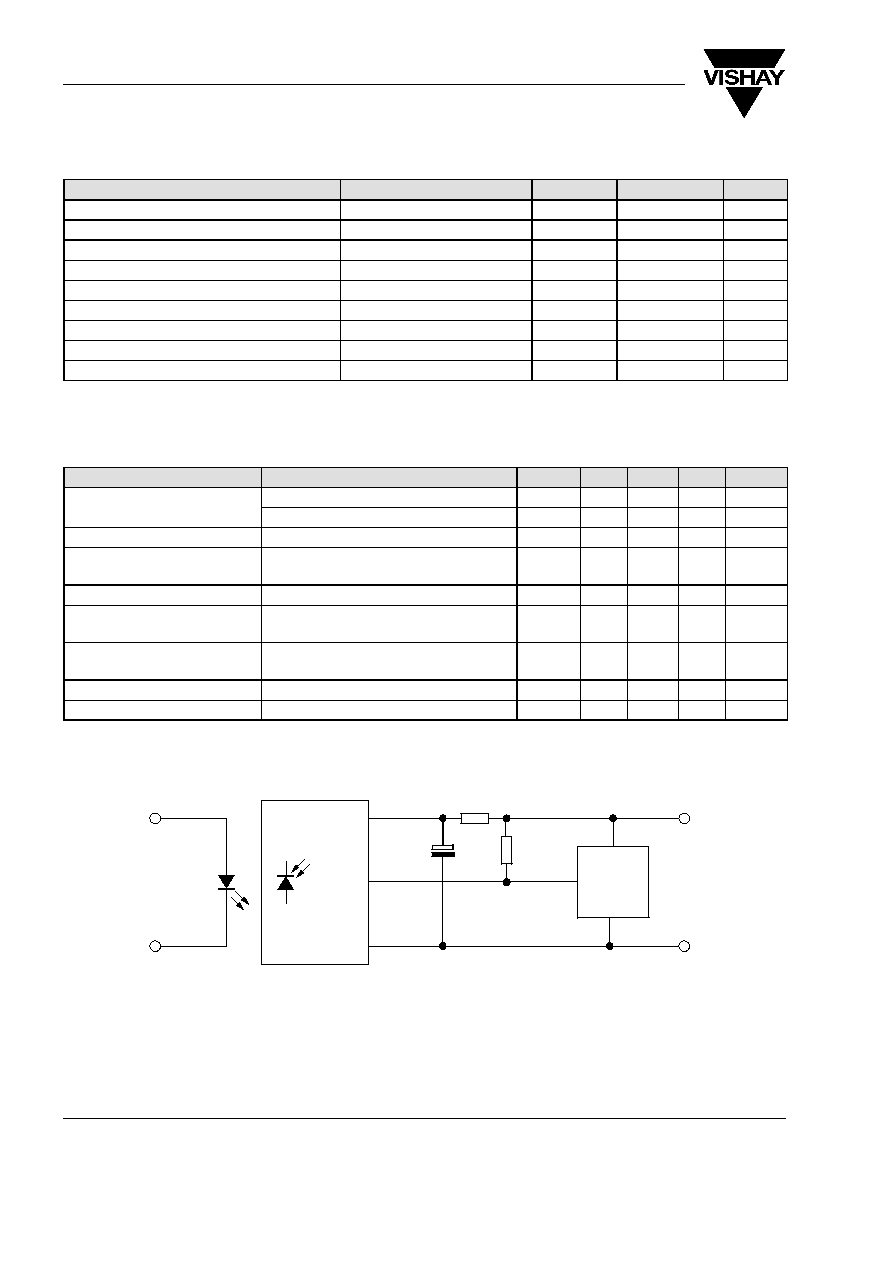
Application Circuit
16238
TSAL62..
TSOP21..YA1
2
1
3
4.7
m
F *)
m
C
>10 k
W
optional
100
W
*)
+ 5 V
*) recommended to suppress power supply disturbances
GND
**) The output voltage should not be hold continuously at a voltage below 3.3V by the external circuit.
**)
TSOP21..YA1
Vishay Telefunken
3 (8)
Rev. 5, 30-Mar-01
www.vishay.com
Document Number 82117
Suitable Data Format
The circuit of the TSOP21..YA1 is designed in that
way that unexpected output pulses due to noise or dis-
turbance signals are avoided. A bandpassfilter, an
integrator stage and an automatic gain control are
used to suppress such disturbances.
The distinguishing mark between data signal and dis-
turbance signal are carrier frequency, burst length and
duty cycle.
The data signal should fullfill the following condition:
·
Carrier frequency should be close to center
frequency of the bandpass (e.g. 38kHz).
·
Burst length should be 6 cycles/burst or longer.
·
After each burst which is between 6 cycles and 70
cycles a gap time of at least 10 cycles is
neccessary.
·
For each burst which is longer than 1.8ms a
corresponding gap time is necessary at some time
in the data stream. This gap time should have at
least same length as the burst.
·
Up to 2200 short bursts per second can be received
continuously.
Some examples for suitable data format are:
NEC Code, Toshiba Micom Format, Sharp Code, RC5
Code, RC6 Code, RCMM Code, R2000 Code,
RECS80 Code.
When a disturbance signal is applied to the
TSOP21..YA1 it can still receive the data signal.
However the sensitivity is reduced to that level that no
unexpected pulses will occure.
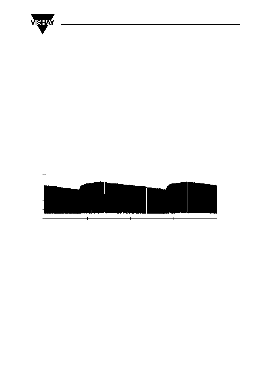
Some examples for such disturbance signals which
are suppressed by the TSOP21..YA1 are:
·
DC light (e.g. from tungsten bulb or sunlight)
·
Continuous signal at 38kHz or at any other
frequency
·
Signals from fluorescent lamps with electronic
ballast (an example of the signal modulation is
shown in the figure below).
0
5
10
15
20
time [ms]
IR Signal from Fluorescent Lamp with low Modulation
TSOP21..YA1
Vishay Telefunken
Rev. 5, 30-Mar-01
www.vishay.com
Document Number 82117
4 (8)
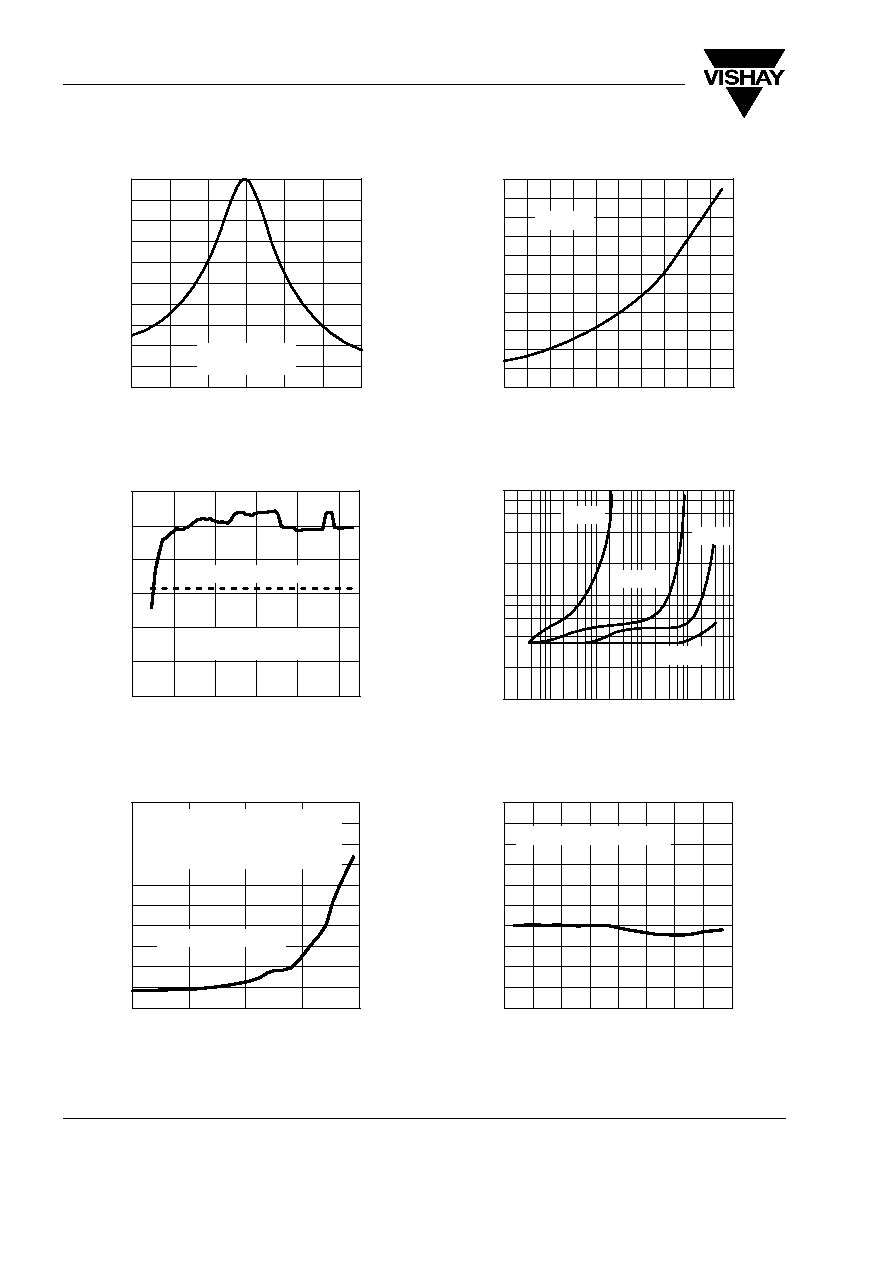
Typical Characteristics (T
amb
= 25
_
C unless otherwise specified)
0.7
0.8
0.9
1.0
1.1
E / E Rel. Responsitivity
e min
f / f
0
Relative Frequency
1.3
94 9102
0.0
0.2
0.4
0.6
0.8
1.0
e
1.2
f = f
0
"5%
Df ( 3dB ) = f
0
/ 7
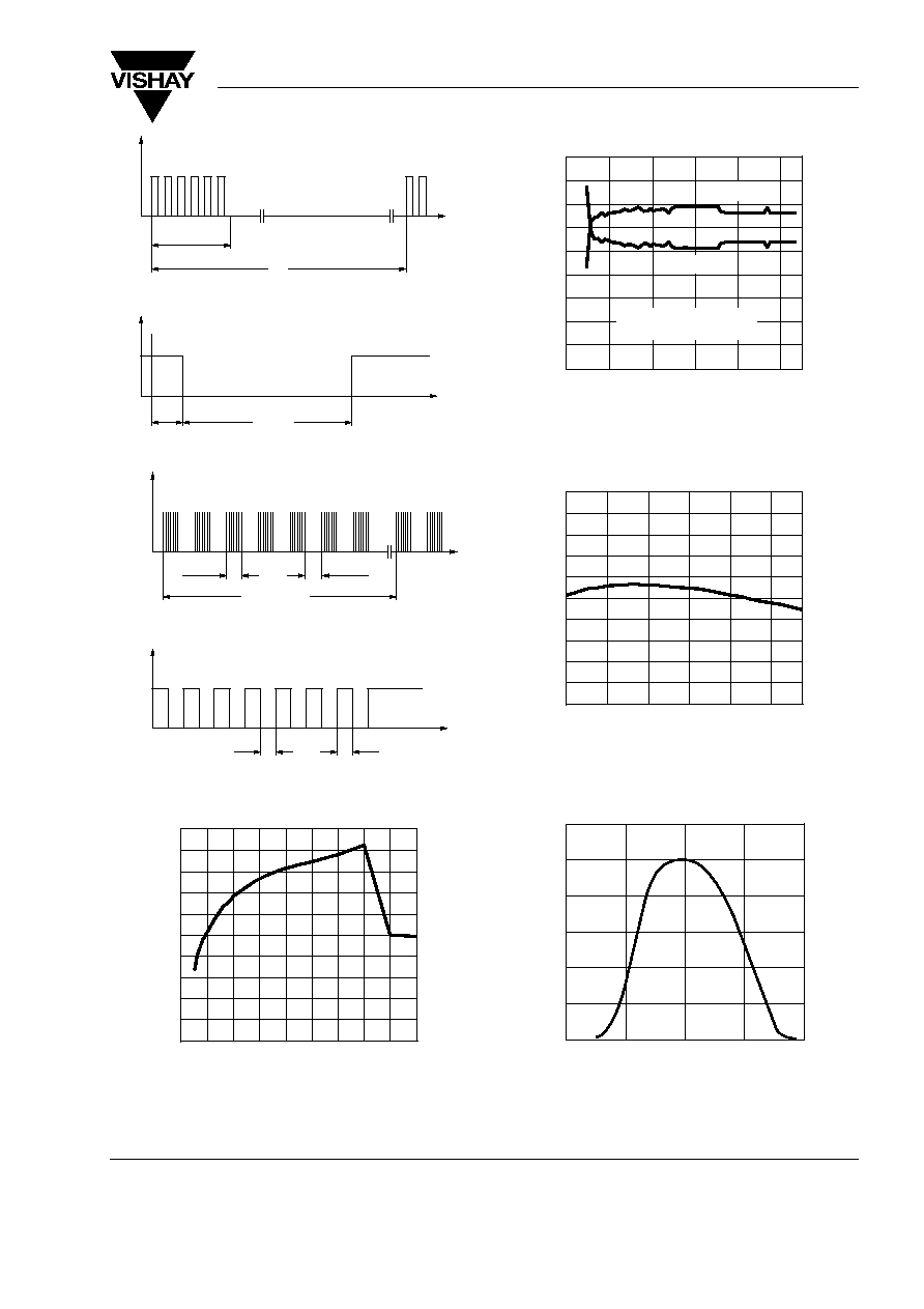
Figure 1. Frequency Dependence of Responsivity
0
0.05
0.10
0.15
0.20
0.25
0.30
0.1
1.0
10.0
100.0
1000.0 10000.0
E
e
Irradiance ( mW/m
2
)
12751
po
t Output Pulse Length (ms)
Input burst duration
l = 950 nm,
optical test signal, fig.7
Figure 2. Pulse Length and Sensitivity in Dark Ambient
0
0.5
1.0
1.5
2.0
2.5
3.0
3.5
4.0
4.5
5.0
0.01
0.10
1.00
10.00
100.00
E DC Irradiance (W/m
2
)
96 12111
e min
E
Threshold
Irradiance
(mW/m
)
2
Correlation with ambient light sources
( Disturbance effect ) : 10W/m
2
^1.4 klx
( Stand.illum.A, T = 2855 K )
^8.2 klx
( Daylight, T = 5900 K )
Ambient,
l = 950 nm
Figure 3. Sensitivity in Bright Ambient
0.0
0.4
0.8
1.2
1.6
0.0
0.4
0.8
1.2
2.0
E Field Strength of Disturbance ( kV / m )
2.0
94 8147
1.6
E
Threshold Irradiance ( mW/m )
e min
2
f ( E ) = f
0
Figure 4. Sensitivity vs. Electric Field Disturbances
0.01
0.1
1
10
100
0.1
1
10
1000
94 9106
DV
s RMS
AC Voltage on DC Supply Voltage ( mV )
E
Threshold Irradiance ( mW/m )
e min
2
f = f
0
10 kHz
100 Hz
1 kHz
Figure 5. Sensitivity vs. Supply Voltage Disturbances
0
0.1
0.2
0.3
0.4
0.5
0.6
0.7
0.8
0.9
1.0
30 15
0
15
30
45
60
75
90
T
amb
Ambient Temperature (
°
C )
96 12112
e min
E
Threshold
Irradiance
(mW/m
)
2
Sensitivity in dark ambient
Figure 6. Sensitivity vs. Ambient Temperature
TSOP21..YA1
Vishay Telefunken
5 (8)
Rev. 5, 30-Mar-01
www.vishay.com
Document Number 82117
E
e
T
tpi
*
t
V
O
V
OH
V
OL
t
po
2 )
t
16298
Optical Test Signal
( IR diode TSAL6200, I
F
=0.4 A, N=6 pulses, f=f
0
, T=10 ms )
Output Signal
t
d
1 )
1 )
3/f
0
< t
d
< 9/f
0
2 )
t
pi
5/f
0
< t
po
< t
pi
+ 5/f
0
* t
pi
w 6/fo is recommended for optimal function
Figure 7. Output Function
E
e
t
V
O
V
OH
V
OL
t
600
ms
600
ms
T = 60 ms
T
on
T
off
94 8134
Optical Test Signal
Output Signal, ( see Fig.10 )
Figure 8. Output Function
0
0.1
0.2
0.3
0.4
0.5
0.6
0.7
0.8
0.9
1.0
0
10
20
30
40
50
60
70
80
90
T
amb
Ambient Temperature (
°
C )
16137
Envelope Duty Cycle
Figure 9. Max. Envelope Duty Cycle vs. Burstlength
0
0.1
0.2
0.3
0.4
0.5
0.6
0.7
0.8
0.9
0.1
1.0
10.0
100.0
1000.0 10000.0
E
e
Irradiance (mW/m
2
)
12753
on of
f
T
,T
Output Pulse Length (ms)
T
on
l = 950 nm,
optical test signal, fig.8
T
off
Figure 10. Output Pulse Diagram
1
1.02
1.04
1.06
1.08
1.10
1.12
1.14
1.16
1.18
1.20
25
5
15
35
55
75
T
amb
Ambient Temperature (
°
C )
16138
I Supply Current ( mA
)
s
Figure 11. Supply Current vs. Ambient Temperature
750
850
950
1050
0
0.2
0.4
0.6
0.8
1.2
S ( ) Relative Spectral Sensitivity
rel
l Wavelength ( nm )
1150
94 8408
1.0
l
Figure 12. Relative Spectral Sensitivity vs. Wavelength