V50100P
Document Number 88929
01-Dec-05
Vishay General Semiconductor
www.vishay.com
1
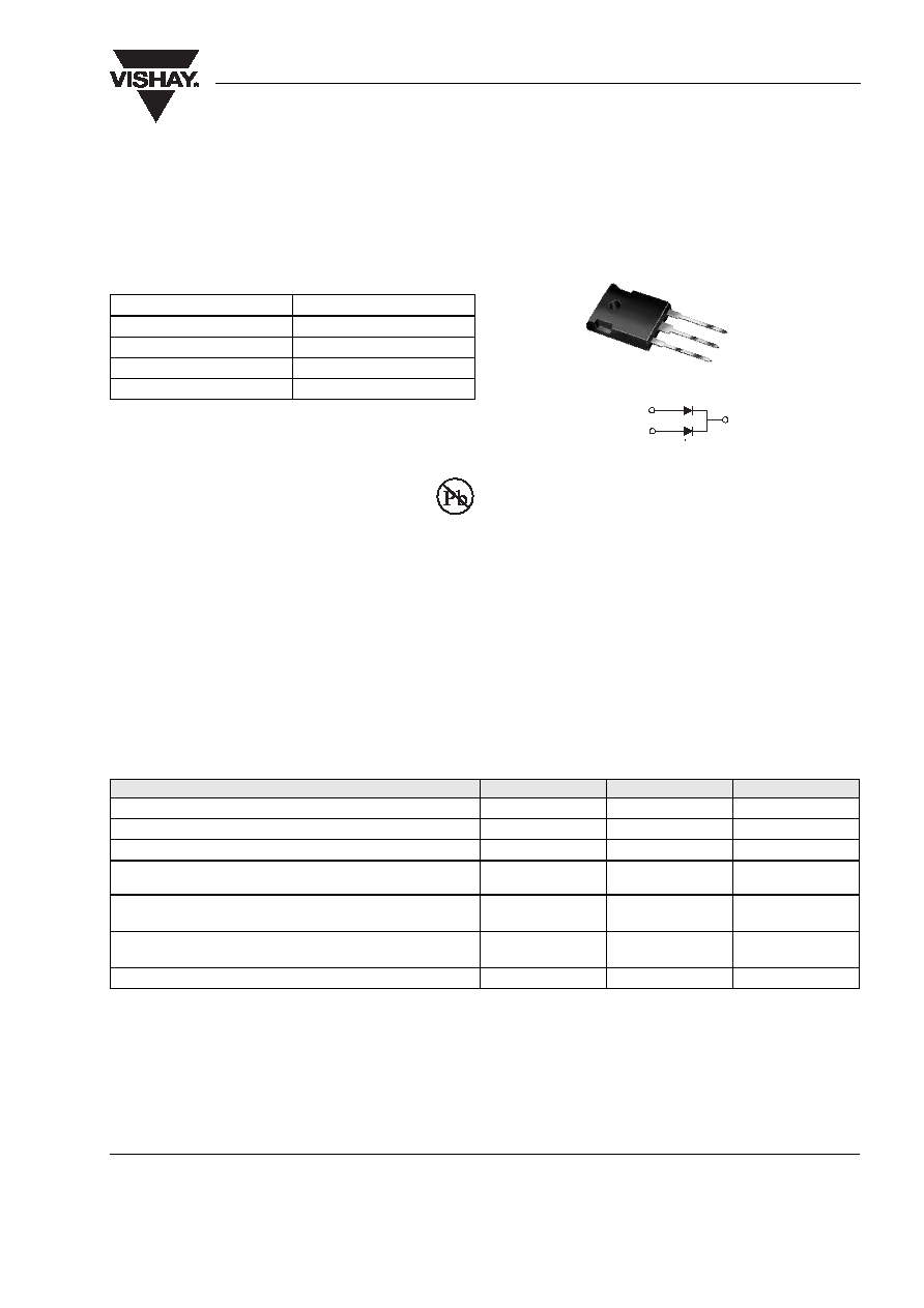
PIN 1
PIN 3
CASE
PIN 2
TO-247AD (TO-3P)
1
2
3
New Product
Dual High-Voltage Trench MOS Barrier Schottky Rectifier
Ultra Low V
F
= 0.372 V at I
F
= 5 A
Major Ratings and Characteristics
I
F(AV)
2 x 25 A
V
RRM
100 V
I
FSM
250 A
V
F
at I
F
= 20 A
0.64 V
T
J
max.
150 �C
Features
� Trench MOS Schottky Technology
� Low forward voltage drop, low power losses
� High efficiency operation
� Low thermal resistance
� Solder Dip 260 �C, 40 seconds
Typical Applications
For use in high frequency inverters, switching power
supplies, freewheeling diodes, Oring diode, dc-to-dc
converters and reverse battery protection.
Mechanical Data
Case: TO-247AD (TO-3P)
Epoxy meets UL 94V-0 flammability rating
Terminals: Matte tin plated leads, solderable per
J-STD-002B and JESD22-B102D
E3 suffix for commercial grade
Polarity: As marked
Mounting Torque: 10 in-lbs Maximum
Maximum Ratings
(T
A
= 25 �C unless otherwise specified)
Parameter
Symbol
V50100P
Unit
Maximum repetitive peak reverse voltage
V
RRM
100
V
RMS reverse voltage for sine wave
V
RMS
70
V
DC blocking voltage
V
R
100
V
Maximum average forward rectified current
(see Fig. 1)
per device
per leg
I
F(AV)
50
25
A
Peak forward surge current 8.3 ms single half
sine-wave superimposed on rated load
per leg
I
FSM
250
A
Peak repetitive reverse current per leg
at t
p
= 2 �s, 1 kHz
I
RRM
1.0
A
Operating junction and storage temperature range
T
J
, T
STG
- 20 to + 150
�C
www.vishay.com
2
Document Number 88929
01-Dec-05
V50100P
Vishay General Semiconductor
Electrical Characteristics
(T
A
= 25 �C unless otherwise specified)
Thermal Characteristics
(T
A
= 25 �C unless otherwise specified)
Notes:
(1) Pulse test: 300 �s pulse width, 1 % duty cycle
Ratings and Characteristics Curves
(T
A
= 25
�C unless otherwise noted)
Parameter
Test condition
Symbol
Typ.
Max.
Unit
Breakdown voltage
at I
R
= 1.0 mA
T
J
= 25 �C
V
(BR)
100 (minimum)
-
V
Instantaneous forward voltage
(1)
per leg
at I
F
= 5 A
I
F
= 10 A
T
J
= 25 �C
V
F
0.463
-
V
0.535
-
I
F
= 20 A
0.664
-
I
F
= 25 A
0.700
0.78
I
F
= 5 A
T
J
= 125 �C
0.375
-
I
F
= 10 A
0.445
-
I
F
= 20 A
0.605
-
I
F
= 25 A
0.635
0.70
Reverse current at rated V
RM
(1)
per leg
at V
R
= 70 V
T
J
= 25 �C
T
J
= 125 �C
I
R
13.7
8.4
500
15
�A
mA
at V
R
= 100 V
T
J
= 25 �C
T
J
= 125 �C
69.6
22.5
1000
45
�A
mA
Parameter
Symbol
V50100P
Unit
Typical thermal resistance per leg
R
JC
1.5
�C/W
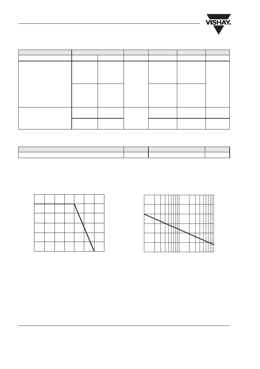
Figure 1. Forward Current Derating Curve
Case Temperature (�C)
60
50
40
30
20
10
0
0
25
50
75
100
125
150
175
A
v
er
age F
o
r
w
ard C
u
rrent (
A)
Figure 2. Maximum Non-Repetitive Peak Forward Surge Current
0
50
100
150
200
250
300
1
10
100
Number of Cycles at 60 Hz
Pe
a
k
F
o
r
w
ard S
u
rge C
u
rrent (A)
V50100P
Document Number 88929
01-Dec-05
Vishay General Semiconductor
www.vishay.com
3
Package outline dimensions in inches (millimeters)
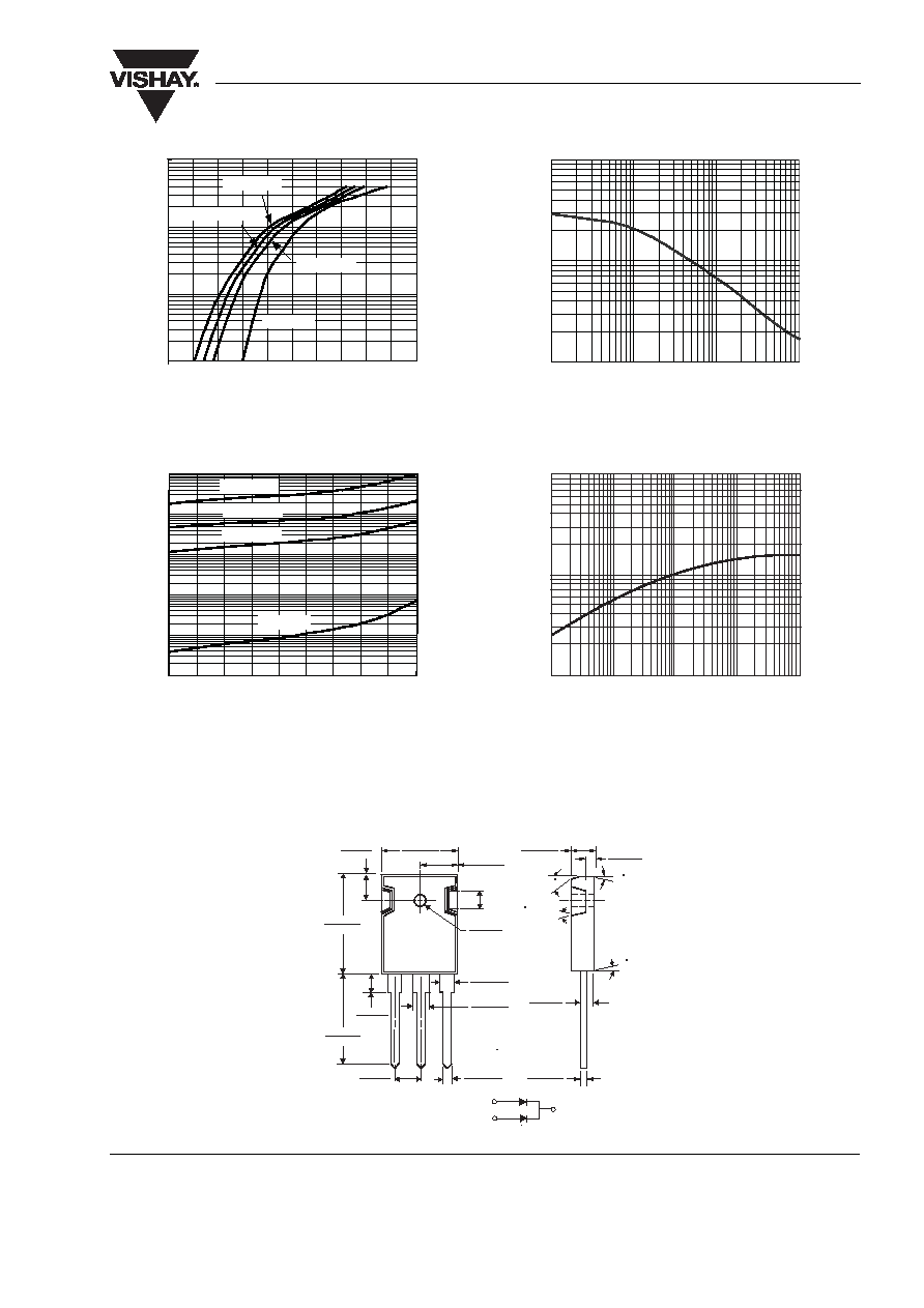
Figure 3. Typical Instantaneous Forward Characteristics Per Leg
Figure 4. Typical Reverse Characteristics
Instantaneo
u
s F
o
r
w
ard C
u
rrent (A)
Instantaneous Forward Voltage (V)
0
0.2
0.4
0.6
0.8
1
100
10
1
0.1
T
J
= 100 �C
T
J
= 150 �C
T
J
= 125 �C
T
J
= 25 �C
10
20
30
40
50
60
70
80
90
100
1
0.1
0.01
0.001
100
10
Percent of Rated Peak Reverse Voltage (%)
Instantaneo
u
s Re
v
erse C
u
rrent (mA)
T
J
= 150 �C
T
J
= 125 �C
T
J
= 100 �C
T
J
= 25 �C
Figure 5. Typical Junction Capacitance
Figure 6. Typical Transient Thermal Impedance
1
10
100
0.1
Reverse Voltage (V)
J
u
nction Capacitance (pF)
10000
1000
100
0.01
0.1
1
10
100
t, Pulse Duration, sec
10
1
0.1
T
r
ansient Ther
mal
Impedance
(�C/
W
)
PIN 1
PIN 3
CASE
0.245 (6.2)
0.225 (5.7)
0.645 (16.4)
0.625 (15.9)
0.323 (8.2)
0.313 (7.9)
0.142 (3.6)
0.138 (3.5)
0.170
(4.3)
0.086 (2.18)
0.076 (1.93)
0.160 (4.1)
0.140 (3.5)
0.225 (5.7)
0.205 (5.2)
0.127 (3.22)
0.117 (2.97)
0.048 (1.22)
0.044 (1.12)
0.795 (20.2)
0.775 (19.6)
0.840 (21.3)
0.820 (20.8)
1
2
3
0.078 REF
(1.98)
0.203 (5.16)
0.193 (4.90)
10 TYP.
BOTH SIDES
30
10
1 REF.
0.118 (3.0)
0.108 (2.7)
0.030 (0.76)
0.020 (0.51)
BOTH
SIDES
PIN 2
TO-247AD (TO-3P)

Legal Disclaimer Notice
Vishay
Document Number: 91000
www.vishay.com
Revision: 08-Apr-05
1
Notice
Specifications of the products displayed herein are subject to change without notice. Vishay Intertechnology, Inc.,
or anyone on its behalf, assumes no responsibility or liability for any errors or inaccuracies.
Information contained herein is intended to provide a product description only. No license, express or implied, by
estoppel or otherwise, to any intellectual property rights is granted by this document. Except as provided in Vishay's
terms and conditions of sale for such products, Vishay assumes no liability whatsoever, and disclaims any express
or implied warranty, relating to sale and/or use of Vishay products including liability or warranties relating to fitness
for a particular purpose, merchantability, or infringement of any patent, copyright, or other intellectual property right.
The products shown herein are not designed for use in medical, life-saving, or life-sustaining applications.
Customers using or selling these products for use in such applications do so at their own risk and agree to fully
indemnify Vishay for any damages resulting from such improper use or sale.