
www.vishay.com
N1
VFC1206
Vishay Foil Resistors
Document Number: 63084
Revision 03-Jul-02
VISHAY FOIL ∑ FRANCE +33.4.93.37.28.24 FAX: +33.4.93.37.27.31
∑ GERMANY +49.9287.710 FAX: +49 9287.70435
∑ ISRAEL +972.3.557.0945 FAX: +972.3.558.9121
∑ ITALY + 39.2.300.11919 FAX: +39.2.300.11999
∑ JAPAN +81.42.729.0661 FAX: +81.42.729.3400
∑ SINGAPORE +65.788.6668 FAX: +65.788.0988
∑ SWEDEN +46.8.594.70590 FAX: +46.8.594.70581
∑ UK +44 191 514 8237 FAX: +44 1953 457 722
∑ USA +1 610 407-4800 FAX: +1 610 640-9081
FEATURES
∑ Nominal TCR: 0.5ppm/
∞
C (- 55
∞
C to + 125
∞
C)
∑ Resistance Range: 10
to 30K
∑ Tolerance: to
±
0.01%
∑ Load Life Stability:
±
0.01% maximum
R under full rated
power at + 70
∞
C for 2000 hours
∑ Shelf Life Stability: 50ppm (0.005%) over several years
∑ Voltage Coefficient: < 0.00001%/volt (< 0.1ppm/V)
∑ Current Noise: < 0.010
µ
V (rms)/volt of applied voltage
∑ Non Inductive: < 0.08
µ
H
TABLE 1 - RESISTANCE VALUE VS
TOLERANCE AND TCR
VALUE
STANDARD
MAXIMUM
TOLERANCE (%)*
TCR**
100
to 30K
±
0.01%
±
2.0ppm/
∞
C
50
to < 100
±
0.05
±
3.0ppm/
∞
C
25
to < 50
±
0.1
±
4.0ppm/
∞
C
10
to < 25
±
0.25
±
5.0ppm/
∞
C
TEST
MIL-PRF-55342
VFC1206
CHARACTERISTIC E MAXIMUM
R LIMITS*
R LIMITS**
Temperature Coefficient of
±
25ppm/
∞
C
See Table 1
Resistance
Thermal Shock
±
0.10%
±
0.02%
Low Temperature Operation
±
0.10%
±
0.02%
Short Time Overload
±
0.10%
±
0.02%
High Temperature Exposure
±
0.10%
±
0.03%
Resistance to Bonding
±
0.20%
±
0.02%
Moisture Resistance
±
0.20%
±
0.03%
Life 2000hrs at + 70
∞
C
±
0.50%
±
0.01%
TABLE 2 - TYPICAL PERFORMANCE SPECIFICATIONS
NOTES:
* As shown + 0.01
to allow for measurement error.
** As shown + 0.01
to allow for measurement error for values less
than 100
.
High Precision Flip Chip,
Patents Pending (Industrialized Countries)
*Tighter tolerances are available. Please contact Application
Engineering.
**Range: - 55
∞
C to + 125
∞
C, + 25
∞
C reference
- 50
- 25
0
+ 25
+ 50
+ 75
+ 100
+ 125
+ 150
+ 100
+ 50
0
- 50
- 100
- 150
- 200
R
R
(PPM)
Ambient Temperature (
∞
C)
FIGURE 1 - NOMINAL TCR
COMPARISON OF Z FOIL TO C FOIL
- 55
The TCR for values < 100
are influenced by the termination
composition and result in a deviation from this curve.
< 0.5PPM/
∞
C
Z Alloy
C Alloy 2PPM/
∞
C
Z Alloy 0.5PPM/
∞
C
< 2PPM/
∞
C
C Alloy
The VFC1206 is a surface mountable flip chip resistor that
utilizes Ultra Precision Bulk Metal
Æ
"Z" Foil. This product differs
from other Vishay Bulk Metal
Æ
Foil surface mount devices in
as much as it is installed with the foil side facing the PCB
providing better power handling capabilities. The Foil
element is isolated from the PCB by a protective overcoating.
This overcoating plus the overall product design isolates the
resistor from handling and installation stresses.
The temperature coefficient of resistance (TCR) curve shown
below compares the new revolutionary "Z" Foil with its TCR of
< 0.5ppm/
∞
C to the original Vishay "C" Foil. The Bulk Metal
Æ
Foil characteristics of excellent long term stability, low noise
and availability of tight tolerance are maintained in this Flip
Chip configuration. The VFC1206 is available in any value
within the specified resistance range. The flip chip configuration
is more economical for high volume, anolog applications where
high precision is required.
Product may not
be to scale
Document Number: 63084
Revision 03-Jul-02
www.vishay.com
N2
VFC1206
Vishay Foil Resistors
VISHAY FOIL ∑ FRANCE +33.4.93.37.28.24 FAX: +33.4.93.37.27.31
∑ GERMANY +49.9287.710 FAX: +49 9287.70435
∑ ISRAEL +972.3.557.0945 FAX: +972.3.558.9121
∑ ITALY + 39.2.300.11919 FAX: +39.2.300.11999
∑ JAPAN +81.42.729.0661 FAX: +81.42.729.3400
∑ SINGAPORE +65.788.6668 FAX: +65.788.0988
∑ SWEDEN +46.8.594.70590 FAX: +46.8.594.70581
∑ UK +44 191 514 8237 FAX: +44 1953 457 722
∑ USA +1 610 407-4800 FAX: +1 610 640-9081
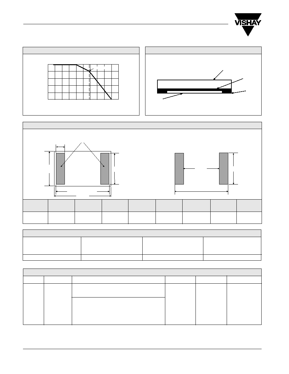
L
W
D
Solder Terminal (2)
High Purity Alumina
Substrate
Resistive
Bulk Metal
Æ
Foil
Solder
Protective
Coating
FIGURE 3 - CHIP CONFIGURATION
MODEL
CHIP SIZE
RESISTANCE VALUE
TOLERANCE
TERMINATION
PACKAGING
VFC
1206
RESISTANCE
LETTER
MULTIPLIER
T
±
0.01%
B - solderable
T = Tape and
RANGE
DESIGNATOR
FACTOR
Q
±
0.02%
Reel
A
±
0.05%
W = Waffle Pack
10
to <1K
R
x 1.0
B
±
0.1%
Example: 249R00 = 249
C
±
0.25%
D
±
0.5%
F
±
1.0%
1K to 30K
K
x 10
3
Example: 10K000 = 10.0K
TABLE 4 - ORDERING INFORMATION
Patent Pending
FIGURE 2 - POWER DERATING CURVE
Bulk Metal
Æ
Foil Technology
High Precision Flip Chip, Patent Pending
Z
G
X
Bottom View (Showing Terminals for Mounting):
FIGURE 4 - DIMENSIONS AND LAND PATTERN
in inches (millimeters)
CHIP
L
W
THICKNESS
D
W1
Z
G
X
SIZE
±
0.005 (0.13)
±
0.005 (0.13)
MAXIMUM
±
0.003 (0.08)
±
0.003 (0.08)
±
0.003 (0.08)
±
0.003 (0.08)
±
0.003 (0.08)
0.126
0.062
0.025
0.015
0.059
0.126
0.090
0.062
1206
(3.20)
(1.57)
(0.64)
(0.38)
(1.50)
(3.20)
(2.29)
(1.57)
Land Pattern
RESISTANCE
POWER
MAXIMUM
MAXIMUM
RANGE
+ 70
∞
C
VOLTAGE
WEIGHT
(
)
(mW)
(V)
(mg)
10R - 30K
125
61
10.3
TABLE 3 - PROPERTIES
125
100
75
50
25
0
-75
≠50
≠25
0
+25
+50
+75
+100 +125 +150 +175
Ambient Temperature (
∞
C)
Percent of Rated Power
≠55
∞
C
+70
∞
C
Rated Power
W1
L - 0.003 (0.08)