 | –≠–ª–µ–∫—Ç—Ä–æ–Ω–Ω—ã–π –∫–æ–º–ø–æ–Ω–µ–Ω—Ç: VSC6464 | –°–∫–∞—á–∞—Ç—å:  PDF PDF  ZIP ZIP |

VITESSE
SEMICONDUCTOR CORPORATION
Advance Product Information
VSC6464
64x64 Crosspoint Switch
G52219-0, Rev. 2.0
©
VITESSE
SEMICONDUCTOR CORPORATION
Page 1
8/4/98
741 Calle Plano, Camarillo, CA 93012 ∑ 805/388-3700 ∑ FAX: 805/987-5896
Features
General Description
The VSC6464 is a 64x64 asynchronous (flow-through) or synchronous (clocked) high-speed crosspoint
switch. Any input can be multiplexed to any, some, or all outputs. The switch is fully non-blocking. All I/Os are
single-ended ECL. The part is packaged in a 208-pin plastic quad flat pack and consumes less than 8 Watts from
a single -2V power supply.
In the asynchronous mode, high speed digital data up to 500Mb/s can be switched with less than 25% pulse
width distortion. Skew is less than 1.5 ns between any two paths through the switch. In broadcast operation (one
input routed to two or more outputs), any two outputs will exhibit less than 750ps of skew.
In the synchronous mode, high-speed digital data up to 250 Mb/s can be switched with less than 750ps out-
put-to-output skew. The input and output registers have separate clock inputs.
VSC6464 Functional Block Diagram
∑ Synchronous or Asynchronous Operation
∑ 500Mb/s Asynchronous Operation
∑ 250Mb/s Synchronous Operation
∑ <750ps Output to Output Skew (Synchronous)
∑ <1.5ns Skew Input to Output (Asynchronous)
∑ Single Ended ECL I/O
∑ Separate Input and Output Register Clocks
∑ Single Supply: -2V + 5% @ 8 Watts (Max.)
∑ Commercial (0
o
to +70
o
C) Temperature Range
∑ Package: 208PQFP
DIN<63:0>
SERC
CKI
REG
DOUT<63:0>
2:1
MUX
REG
2:1
MUX
64 x 64:1
MUX
CKO
SERD
SERS
MODE
SERIAL
TO
PARALLEL
64 6-BIT
REGISTERS
DEC

VITESSE
SEMICONDUCTOR CORPORATION
Advance Product Information
VSC6464
64x64 Crosspoint Switch
Page 2
©
VITESSE
SEMICONDUCTOR CORPORATION
G52219-0, Rev. 2.0
741 Calle Plano, Camarillo, CA 93012 ∑ 805/388-3700 ∑ FAX: 805/987-5896
8/4/98
Functional Description
This Crosspoint Switch connects any of the 64 inputs to any combination of 64 output channels, according
to a user defined bit pattern stored in each channel's control register.
Signals from the 64 inputs (DIN_0 through DIN_63) are connected to the 64 output channels (DOUT_0
through DOUT_63) through sixty-four 64:1 multiplexers. The traffic pattern is controllable by data stored in
sixty-four 6-bit control registers with each register corresponding to an output channel. The six bits are a binary
numerical representation of the input channel selected (i.e.: 000000 corresponds to DIN_0, 000001 corresponds
to DIN_1, etc.). An additional six bit register is used to address the output channel being programmed. These six
bits are a binary numerical representation of the output channel (ie.: 000000 corresponds to DOUT_0, 000001
corresponds to DOUT_1, etc.). All twelve configuration bits are loaded through a three-pin serial port.
The crosspoint is configured through a serial data port consisting of three pins: SERS, SERC, and SERD.
SERS is used to select the crosspoint for configuration. SERC is a serial clock signal whose rising edge samples
the serial data on SERD when SERS is active (HI). The serial data stream applied to SERD consists of the six
bits of address, followed by the six bits of data. Address information is used to identify one of the 64 output
channels, a valid value is between 0 and 63. Data information selects a specific input to be directed to the
addressed output, valid values are between 0 and 63. Both address and data information are received MSB first.
A serial load cycle consists of activating serial select (SERS), pulsing serial clock 12 times (with valid data sur-
rounding each rising edge), then deactivating serial select (SERS). Deactivating serial select before the twelfth
rising edge of SERC will abort the load cycle. Serial select (SERS) must be deactivated for 10ns following a
power up. Any additional clocking of SERC during a load cycle, beyond that described above, is ignored.
The MODE pin determines the operating mode of the Crosspoint: synchronous or asynchronous, as shown
in Table 1.
A test output (TESTO) is provided for internal visibility, this signal will go high when a thirteenth rising
edge is applied during a load cycle; TESTO goes low when either SERS is lowered, or a fourteenth SERC edge
is received during a load cycle. This output can be left unconnected if desired, to reduce noise and power dissi-
pation.
Table 1: Crosspoint Mode (MODE)
Function
MODE
Asynchronous 64x64
0
Synchronous 64x64
1
VITESSE
SEMICONDUCTOR CORPORATION
Advance Product Information
VSC6464
64x64 Crosspoint Switch
G52219-0, Rev. 2.0
©
VITESSE
SEMICONDUCTOR CORPORATION
Page 3
8/4/98
741 Calle Plano, Camarillo, CA 93012 ∑ 805/388-3700 ∑ FAX: 805/987-5896
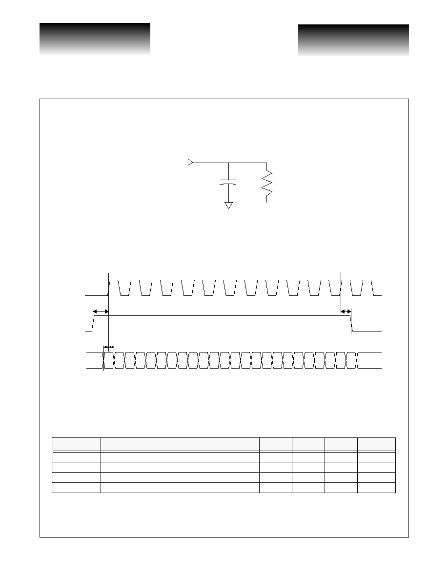
AC Characteristics
(Over recommended operating conditions)
Figure 1 Output Loading
Figure 2 VSC6464 Configuration Timing Diagram
Table 2: VSC6464 Asynchronous Timing Table
Parameters
Description
Min
Typ
Max
Units
T
SS
SERS setup time with respect to SERC
10
-
-
ns
T
SH
SERS hold time with respect to SERC
10
-
-
ns
T
DS
SERD setup time with respect to SERC
10
-
-
ns
T
DH
SERD setup time with respect to SERC
10
-
-
ns
V
TT
50
4pF
Output
SERC
TSS
A5
SERS
Note: A5 is MSB of A<5:0>, D5 is MSB of D<5:0>.
SERD
A4
A3
A2
A1
A0
D5
D4
D2
D1
D0
D3
TSH
TDH
TDS

VITESSE
SEMICONDUCTOR CORPORATION
Advance Product Information
VSC6464
64x64 Crosspoint Switch
Page 4
©
VITESSE
SEMICONDUCTOR CORPORATION
G52219-0, Rev. 2.0
741 Calle Plano, Camarillo, CA 93012 ∑ 805/388-3700 ∑ FAX: 805/987-5896
8/4/98
Figure 3 VSC6464 Asynchronous Timing Diagram
Table 3: VSC6464 Asynchronous Timing Table
Note: 1.) Duty cycle distortion = (duty cycle in - duty cyle out)/duty cycle in * 100%, measured with a 2ns pulse width.
Figure 4 VSC6464 Synchronous Data Input Timing Diagram
Table 4: VSC6464 Synchronous Data Input Timing Table
Parameters
Description
Min
Typ
Max
Units
T
PW
Minimum DIN<63:0> pulse width, 50% input
1.25
-
-
ns
T
AMX
DIN<63:0> to DOUT<63:0> propagation delay
-
-
6.5
ns
T
AMN
DIN<63:0> to DOUT<63:0> propagation delay
2.2
-
-
ns
T
ASKW
DOUT<63:0> asynchronous mode data skew (any input
to any output, add 0.1 for SSO)
-
-
1.4
ns
T
ASKW
DOUT<63:0> asynchronous mode data skew (broadcast,
add 0.1 for SSO)
-
-
0.75
ns
-
Duty Cycle Distortion, @500Mb/s
(1)
-
-
25
%
Parameters
Description
Min
Typ
Max
Units
F
MAX
Maximum CKI frequency, 50% input
-
-
250
MHz
T
INSU
DIN<63:0> data setup time with respect to CKI
0.5
-
-
ns
T
INH
DIN<63:0> data hold time with respect to CKI
0.4
-
-
ns
DOUT<63:0>
DIN<63:0>
TASKW
TAMX
TPW
TAMN
TINSU TINH
DIN<63:0>
CKI

VITESSE
SEMICONDUCTOR CORPORATION
Advance Product Information
VSC6464
64x64 Crosspoint Switch
G52219-0, Rev. 2.0
©
VITESSE
SEMICONDUCTOR CORPORATION
Page 5
8/4/98
741 Calle Plano, Camarillo, CA 93012 ∑ 805/388-3700 ∑ FAX: 805/987-5896
Figure 5 VSC6464 Synchronous Data Output Timing Diagram
Table 5: VSC6464 Synchronous Data Output Timing Table
Figure 6 VSC6464 Synchronous Mode Clock Relationship
Table 6: VSC6464 Synchronous Data Output Timing Table
Note: A nominal delay of 0.25 ns between input and output clocks can be achieved by a trace on the pc board run directly from
the input clock pin to the output clock pin. In this case, the clock signal should be connected to the input pin with the delay
supplied by the pc board trace.
Parameters
Description
Min
Typ
Max
Units
F
MAX
Maximum CKO frequency, 50% input
-
-
250
MHz
T
SMX
Maximum propagation delay CKO toDOUT<63:0>
-
-
3.7
ns
T
SMN
Minimum propagation delay CKO to DOUT<63:0>
1.4
-
-
ns
T
SSKW
DOUT<63:0> synchronous mode data skew
(add 0.1 for SSO)
-
-
0.75
ns
Parameters
Description
Min
Typ
Max
Units
T
CC
CKO relative to CKI, 50% input
0.1
-
0.8
ns
TSSKW
TSMX
DOUT<63:0>
CKO
TSMN
CKI
CKO
TCC
T