 | –≠–ª–µ–∫—Ç—Ä–æ–Ω–Ω—ã–π –∫–æ–º–ø–æ–Ω–µ–Ω—Ç: VSC7122QM | –°–∫–∞—á–∞—Ç—å:  PDF PDF  ZIP ZIP |

©
VITESSE
SEMICONDUCTOR CORPORATION
Page 1
8/31/98
741 Calle Plano, Camarillo, CA 93012 ∑ 805/388-3700 ∑ FAX: 805/987-5896
VITESSE
SEMICONDUCTOR CORPORATION
Advance Product Information
VSC7122
Quad Port Bypass Circuit for 1.0625 Gbit/sec
Fibre Channel Arbitrated Loop Disk Arrays
G52155-0, Rev. 2.1
Features
General Description
The VSC7122 is a Quad Port Bypass Circuit (PBC). Four Fibre Channel PBC's are cascaded into a single
part to minimize part count, cost, high frequency routing, and jitter accumulation. Port Bypass Circuits are used
to provide resiliency in Fibre Channel Arbitrated Loop (FC-AL) architectures. PBC's are used within FC-AL
disk arrays to allow for resiliency and hot swapping of FC-AL drives.
A Port Bypass Circuit is a 2:1 Multiplexer with two modes of operation: NORMAL and BYPASS. In NOR-
MAL mode, the disk drive is connected to the loop. Data goes from the 7122's L_SOn pin to the Disk Drive RX
input and data from the disk drive TX output goes to the 7122's L_SIn pin. Refer to Figure 2 for disk drive
application. In BYPASS mode, the disk drive is either absent or non-functional and data bypasses to the next
available disk drive. Normal mode is enabled with a HIGH on the SEL pin and BYPASS mode is enabled by a
LOW on the SEL pin. Direct Attach Fibre Channel Disk Drives have an "LRC Interlock" signal defined to con-
trol the SEL function.
Using a VSC7122 in a single loop of a disk array is illustrated in Figure 2: "Disk Array Application". FC-
AL drives are all expected to be dual loop. The VSC7122 is cascaded in a manner such that all the 7122's inter-
nal PBC's are used in the same loop. For dual loop implementations, two or more VSC7122's should be used.
Allocating each VSC7122 to only one of two loops preserves redundancy, prevents a single point of failure and
lends itself to on-line maintainability.
The VSC7122 is very similar to the VSC7121 except that LSO+ outputs are all full power outputs identical
to OUT. This is useful in passive backplanes to provide additional amplitude on long traces.
7122 Block Diagram
∑ Supports ANSI X3T11 1.0625 Gbit/sec
FC-AL Disk Attach for Resiliency
∑ Fully Differential for Minimum
Jitter Accumulation.
∑ Quad PBC's in Single Package
∑ TTL Bypass Select
∑ High Speed, PECL I/O's Referenced to V
DD
.
∑ 0.35W Typical Power Dissipation
∑ 3.3V Power Supply
∑ 44-Pin, 10mm PQFP
LSI1+
LSI1-
LSO1+
LSO1-
IN+
IN-
OUT+
OUT-
SEL1
LSI2+
LSI2-
LSO2+
LSO2-
SEL2
LSI3+
LSI3-
LSO3+
LSO3-
SEL3
LSI4+
LSI4-
LSO4+
LSO4-
SEL4
1
0
0
1
0
1
0
1
PBC1
PBC2
PBC3
PBC4
VITESSE
SEMICONDUCTOR CORPORATION
Advance Product Information
VSC7122
Quad Port Bypass Circuit for 1.0625 Gbit/sec
Fibre Channel Arbitrated Loop Disk Arrays
Page 2
©
VITESSE
SEMICONDUCTOR CORPORATION
741 Calle Plano, Camarillo, CA 93012 ∑ 805/388-3700 ∑ FAX: 805/987-5896
8/31/98
G52155-0, Rev. 2.1
The VSC7122 can be cascaded through the IN and OUT pins for arrays of disk drives greater than 4. For
disk arrays with a noninteger multiple of 4 disk drives, the unused PBC's can be hardwired to bypass with a
external pulldown resistor.
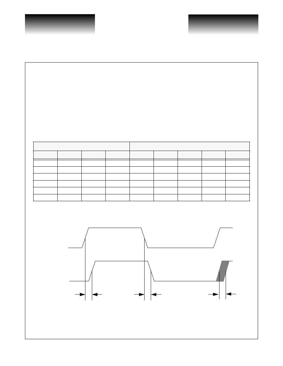
Table 1 is a truth table detailing the data flow through the VSC7122. Figure 1 shows a timing diagram of the
data relationship in the VSC7122. There are no critical timing (setup, hold, or delay) parameters for the
VSC7122 as this part routes the serial data encoded with the baud clock that is extracted by a Fibre Channel
receiver. The primary AC parameter of importance is the jitter or data eye degradation inserted by the port
bypass circuit. The design of the VSC7122 minimizes jitter accummulation by using fully differential circuits.
This provides for symmetric rise and fall delays as well as noise rejection.
Table 1: Truth Table
Figure 1: Timing Waveforms
SELECT STATE
DATA OUTPUTS
SEL1
SEL2
SEL3
SEL4
OUT
SO4
SO3
SO2
SO1
L
L
L
L
IN
IN
IN
IN
IN
L
L
L
H
SI4
IN
IN
IN
IN
L
L
H
L
SI3
SI3
IN
IN
IN
L
H
L
L
SI2
SI2
SI2
IN
IN
H
L
L
L
SI1
SI1
SI1
SI1
IN
H
H
H
H
SI4
SI3
SI2
SI1
IN
T
1
T
2
T
jitter
OUT+/-
LSO1+/-
LSO2+/-
LSO3+/-
LSO4+/-
IN+/-
LSI1+/-
LSI2+/-
LSI3+/-
LSI4+/-

©
VITESSE
SEMICONDUCTOR CORPORATION
Page 3
8/31/98
741 Calle Plano, Camarillo, CA 93012 ∑ 805/388-3700 ∑ FAX: 805/987-5896
VITESSE
SEMICONDUCTOR CORPORATION
Advance Product Information
VSC7122
Quad Port Bypass Circuit for 1.0625 Gbit/sec
Fibre Channel Arbitrated Loop Disk Arrays
G52155-0, Rev. 2.1
Figure 2: Disk Array Application
0
1
0
1
0
1
0
1
RX
TX
E_STORE
LRC Interlock
FC-AL DISK DRIVE
RX
TX
E_STORE
LRC Interlock
FC-AL DISK DRIVE
VSC7122 Q
U
AD POR
T BYP
ASS CIRCUIT
RX
TX
E_STORE
LRC Interlock
FC-AL DISK DRIVE
Pulldown for Bypass
in Absense of Disk Drive
7120
7120
Optics
or
Copper
JBOD
normal
normal
normal
bypass
Dual SC
or
DB-9
7120
7120
VITESSE
SEMICONDUCTOR CORPORATION
Advance Product Information
VSC7122
Quad Port Bypass Circuit for 1.0625 Gbit/sec
Fibre Channel Arbitrated Loop Disk Arrays
Page 4
©
VITESSE
SEMICONDUCTOR CORPORATION
741 Calle Plano, Camarillo, CA 93012 ∑ 805/388-3700 ∑ FAX: 805/987-5896
8/31/98
G52155-0, Rev. 2.1
Table 2: AC Characteristics
(Over recommended operating conditions).
Table 3: DC Characteristics
(Over recommended operating conditions).
Parameters
Description
Min.
Max.
Units
Conditions
T
1
Flow-Through Propagation Delay
Rising Edge to Rising Edge
7.0
ns
Delay with all circuits bypassed. 75
Ohm Load
T
2
Flow through Propagation Delay
Falling Edge to Falling Edge
7.0
ns
Delay with all circuits bypassed. 75
Ohm load.
T
SDR
, T
SDF
Serial data rise and fall time
--
300
ps.
20% to 80%, tested on a sample basis
Parameters
Description
Min
Typ
Max
Units
Conditions
V
IH(TTL)
Input HIGH voltage (SEL - TTL)
2.0
--
5.5
V
I
IH
< 6.6 mA @ V
IH
= 5.5 V
V
IL(TTL)
Input LOW voltage (SEL - TTL)
0
--
0.8
V
--
I
IH(TTL)
Input HIGH current (SEL- TTL)
--
50
500
µ
A
V
IN
= 2.4 V
I
IL(TTL)
Input LOW current (SEL - TTL)
--
--
-500
µ
A
V
IN
= 0.5 V
V
DD
Supply voltage
3.10
--
3.50
V
V
DD
= 3.30V + 5%
I
DD
Supply current
--
--
150
mA
Outputs open, V
DD
= V
DD
max
P
D
Power Dissipation
0.35
0.5
W
Outputs open, V
DD
= V
DD
max
V
IN
Receiver differential peak-to-peak
Input Sensitivity, IN+/- & L_SIn+/-
300
2600
mVp-p
AC Coupled.
Internally biased at V
DD
/2
V
OUT50
Output differential peak-to-peak
voltage swing
1000
--
2200
mVp-p
50
to V
DD
≠ 2.0 V
V
OUT75
Output differential peak-to-peak
voltage swing
1200
2200
mVp-p
75
to V
DD
≠ 2.0 V

©
VITESSE
SEMICONDUCTOR CORPORATION
Page 5
8/31/98
741 Calle Plano, Camarillo, CA 93012 ∑ 805/388-3700 ∑ FAX: 805/987-5896
VITESSE
SEMICONDUCTOR CORPORATION
Advance Product Information
VSC7122
Quad Port Bypass Circuit for 1.0625 Gbit/sec
Fibre Channel Arbitrated Loop Disk Arrays
G52155-0, Rev. 2.1
Absolute Maximum Ratings
(1)
TTL Power Supply Voltage, (V
DD
) ..................................................................................................... 0.5V to +4V
PECL DC Input Voltage, (V
INP
)............................................................................................. -0.5V to V
DD
+0.5V
TTL DC Input Voltage, (V
INT
) .......................................................................................................... -0.5V to 5.5V
DC Voltage Applied to Outputs for High Output State, (V
IN TTL
) ........................................ -0.5V to V
DD
+ 0.5V
TTL Output Current (I
OUT
), (DC, Output High)........................................................................................... 50mA
PECL Output Current, (I
OUT
), (DC, Output High) ......................................................................................-50mA
Case Temperature Under Bias, (T
C
) ............................................................................................... -55
∞
to +125
o
C
Storage Temperature, (T
STG
)......................................................................................................... -65
∞
to + 150
o
C
Maximum Input ESD .................................................................................................................................. 1500 V
Recommended Operating Conditions
(2)
Power Supply Voltage, (V
DD
) ...........................................................................................................+3.1V to 3.5V
Ambient Operating Temperature Range, (T) .....................................................................................0
∞
C to +70
∞
C
Notes:
1)
CAUTION: Stresses listed under "Absolute Maximum Ratings" may be applied to devices one at a time without causing per-
manent damage. Functionality at or above the values listed is not implied. Exposure to these values for extended periods may
affect device reliability.
2)
Vitesse guarantees the functional and parametric operation of the part under "Recommended Operating Conditions: except
where specifically noted in the AC and DC Parametric Tables

VITESSE
SEMICONDUCTOR CORPORATION
Advance Product Information
VSC7122
Quad Port Bypass Circuit for 1.0625 Gbit/sec
Fibre Channel Arbitrated Loop Disk Arrays
Page 6
©
VITESSE
SEMICONDUCTOR CORPORATION
741 Calle Plano, Camarillo, CA 93012 ∑ 805/388-3700 ∑ FAX: 805/987-5896
8/31/98
G52155-0, Rev. 2.1
Input Structures
Two input structures exist in this part; TTL and High Speed, Differential Inputs. The TTL Inputs will inter-
face with any TTL or 3.3V or 5V CMOS outputs. The High Speed, Differential Inputs are intended to be AC
Coupled per the FC-PH specification. Being AC Coupled, the High Speed, Differential Input buffers are biased
at V
DD
/2. Refer to Figure 3 for High Speed, Differential Input structure.
Figure 3: High Speed, Differential Inputs (L_SIn/IN)
Because the VSC7122 output buffers are PECL outputs referenced to V
DD
, the High Speed Differential out-
puts may not be direct coupled to the high speed differential inputs. One example of how to differentially cas-
cade the two VSC7122 is shown in Figure 4.
Figure 4: Cascading Two VSC7122
INPUT+
INPUT-
VDD/2
3.3K
3.3K
VDD
GND
0 V
+3.3 V
3.3K
3.3K
VSC7122
OUT+
OUT -
VSC7122
IN+
IN -
V
DD
191
124
124
191
.01
75 Ohm Board/Termination Example
.01
©
VITESSE
SEMICONDUCTOR CORPORATION
Page 7
8/31/98
741 Calle Plano, Camarillo, CA 93012 ∑ 805/388-3700 ∑ FAX: 805/987-5896
VITESSE
SEMICONDUCTOR CORPORATION
Advance Product Information
VSC7122
Quad Port Bypass Circuit for 1.0625 Gbit/sec
Fibre Channel Arbitrated Loop Disk Arrays
G52155-0, Rev. 2.1
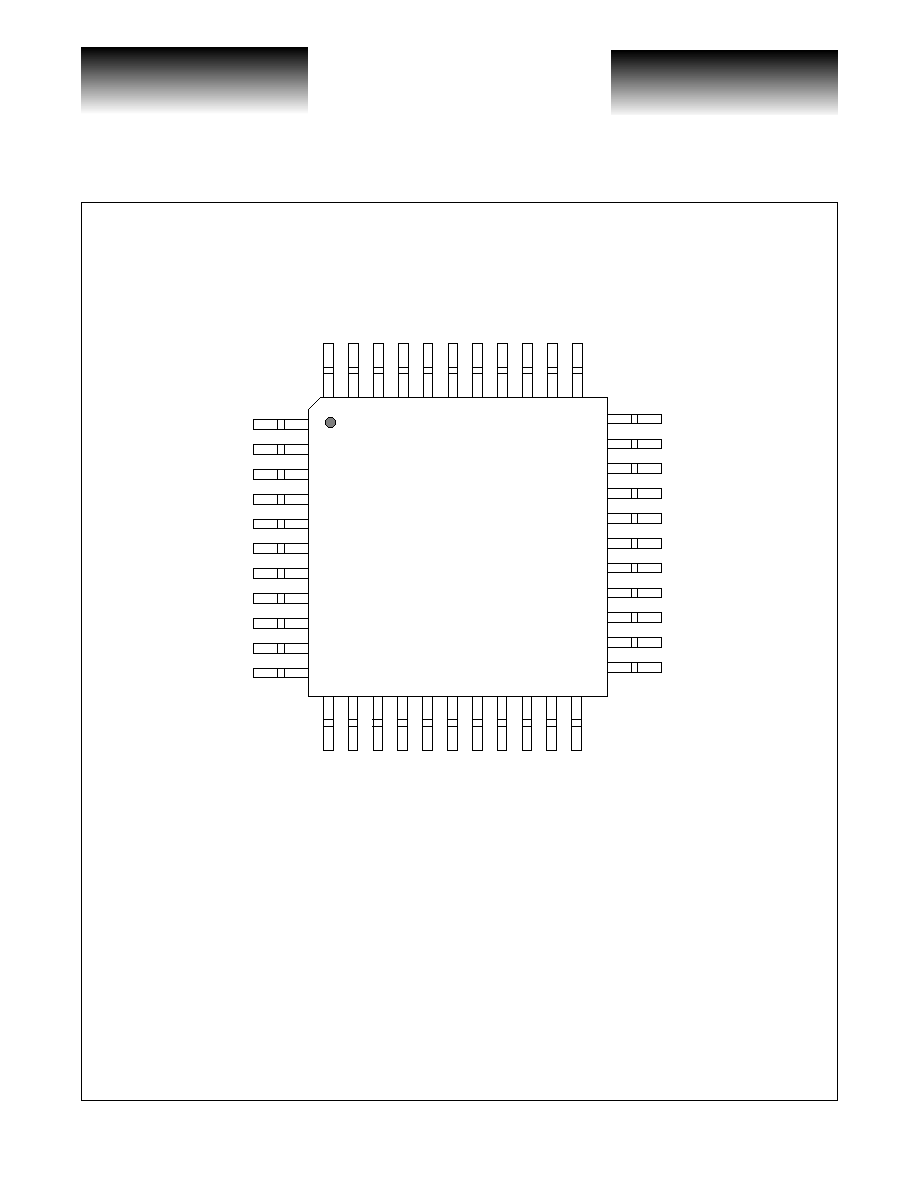
Figure 5: Pin Diagram
VSS
VSS
IN+
VSS
L_SO2+
L_SO3-
L_SO2-
VDDP
L_SI3+
VSS
OUT+
L_SO4+
OUT-
VDDP
L_SO1-
L_SO1+
VDD
L_SI4-
VDD
VSS
VSS
SEL4
VDD
IN-
VSS
VSS
SEL3
SEL1
SEL2
VDD
VDDP
L_SI4+
VDDP
L_SO4-
VDD
L_SI2-
L_SI2+
L_SI1+
L_SI1-
VSS
L_SO3+
L_SI3-
VDDP
VSC7122
VSS
1
3
5
7
9
11
33
31
29
27
25
23
13
15
17
19
21
43
41
39
37
35

VITESSE
SEMICONDUCTOR CORPORATION
Advance Product Information
VSC7122
Quad Port Bypass Circuit for 1.0625 Gbit/sec
Fibre Channel Arbitrated Loop Disk Arrays
Page 8
©
VITESSE
SEMICONDUCTOR CORPORATION
741 Calle Plano, Camarillo, CA 93012 ∑ 805/388-3700 ∑ FAX: 805/987-5896
8/31/98
G52155-0, Rev. 2.1
Table 4: Pin Description
Pin #
Name
Description
9, 10
IN-, IN+
INPUT - Differential (Biased at VDD/2). Serial inputs from the downstream PBC port.
3, 4
L_SI1-, L_SI1+
INPUT - Differential (Biased at VDD/2). Serial input from the local transmitter on PBC
port 1.
40, 41
L_SI2-, L_SI2+
INPUT - Differential (Biased at VDD/2). Serial input from the local transmitter on PBC
port 2.
34, 35
L_SI3-, L_SI3+
INPUT - Differential (Biased at VDD/2). Serial input from the local transmitter on PBC
port 3.
27, 28
L_SI4-, L_SI4+
INPUT - Differential (Biased at VDD/2). Serial input from the local transmitter on PBC
port 4.
15-18
SEL1, SEL2,
SEL3, SEL4
INPUT - TTL. A LOW selects the "BYPASS" mode causing the output of the previous
port to propagate to next port or OUT. When HIGH, this signal selects "NORMAL"
mode which routes the previous port to the local output, L_SOn, and routes the local
input, L_SIn, to the next port or OUT .
6, 7
L_SO1-,
L_SO1+
OUTPUT - Differential Serial output driving the local receiver corresponding to PBC
port 1.
43, 44
L_SO2-,
L_SO2+
OUTPUT - Differential Serial output driving the local receiver corresponding to PBC
port 2.
37, 38
L_SO3-,
L_SO3+
OUTPUT - Differential Serial output driving the local receiver corresponding to PBC
port 3.
30, 31
L_SO4-,
L_SO4+
OUTPUT - Differential Serial output driving the local receiver corresponding to PBC
port 4.
25, 24
OUT-, OUT+
OUTPUT - Differential Serial output driving the upstream PBC port.
2, 14, 20-21,
32
VDD
Digital Logic Power Supply. 3.3V Supply for digital logic.
5, 26, 29 36,
42
VDDP
High-Speed Output Power Supply. 3.3V Supply for PECL drivers.
1, 8, 11-13,
19, 22-23,
33, 39
VSS
Ground. Ground pins are physically attached to the die mounting surface, and are an
important part of the thermal path. For best thermal performance, all ground pins should
be connected to a ground plane, using multiple vias if possible.

©
VITESSE
SEMICONDUCTOR CORPORATION
Page 9
8/31/98
741 Calle Plano, Camarillo, CA 93012 ∑ 805/388-3700 ∑ FAX: 805/987-5896
VITESSE
SEMICONDUCTOR CORPORATION
Advance Product Information
VSC7122
Quad Port Bypass Circuit for 1.0625 Gbit/sec
Fibre Channel Arbitrated Loop Disk Arrays
G52155-0, Rev. 2.1
Package Information
44
34
0.102 MAX. LEAD
COPLANARITY
1
33
23
22
12
G
F
I
H
12
o
TYP
0.17 MAX.
NOTES:
12
o
TYP
K
D
A
0.25
J
0
o
- 8
o
0.25 MAX.
E
0.30 RAD. TYP.
0.20 RAD. TYP.
11
Drawing not to scale.
Cavity up
All units in mm unless otherwise noted.
Item
mm
Tol.
A
2.35
MAX
D
2.00
+0.10
E
0.35
+.05
F
13.20
+.25
G
10.00
+.10
H
13.20
+.25
I
10.00
+.10
J
0.8
+.15 / -.10
K
0.80
BASIC
44-Pin PQFP 10 x 10 mm
VITESSE
SEMICONDUCTOR CORPORATION
Advance Product Information
VSC7122
Quad Port Bypass Circuit for 1.0625 Gbit/sec
Fibre Channel Arbitrated Loop Disk Arrays
Page 10
©
VITESSE
SEMICONDUCTOR CORPORATION
741 Calle Plano, Camarillo, CA 93012 ∑ 805/388-3700 ∑ FAX: 805/987-5896
8/31/98
G52155-0, Rev. 2.1
Package Thermal Characteristics
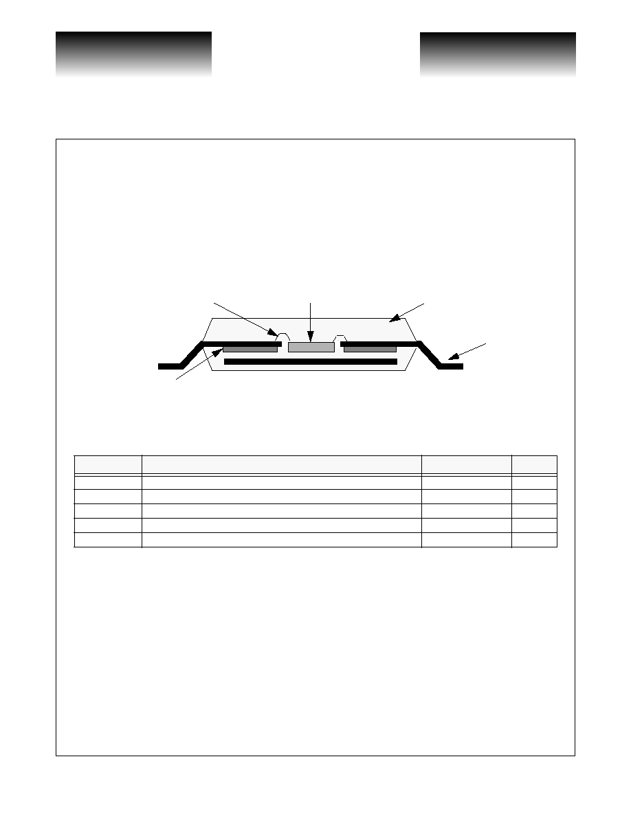
The VSC7122 is packaged into a standard plastic quad flatpack with an embedded, but unexposed thermal
slug. This package adheres to industry standard EIAJ footprints for a 10x10mm body, 44 lead PQFP. The pack-
age construction is as shown in Figure 6. The 44 PQFP with embedded slug has the thermal properties shown in
Table 5. This package allows the VSC7122 to operate with ambient temperatures up to 70
o
C in still air.
Figure 6: Package Cross Reference
Table 5: 44 PQFP Thermal Resistance
Moisture Sensitivity Level
This device is rated with a moisture sensitivity level 3 rating. Refer to Application Note AN-20 for appro-
priate handling procedures.
Symbol
Description
Value
Units
ca-0
Thermal resistance from case to ambient, still air
50
o
C/W
ca-100
Thermal resistance from case to ambient, 100 LFPM air
43
o
C/W
ca-200
Thermal resistance from case to ambient, 200 LFPM air
39
o
C/W
ca-400
Thermal resistance from case to ambient, 400 LFPM air
36
o
C/W
ca-600
Thermal resistance from case to ambient, 600 LFPM air
34
o
C/W
Lead
Die
Plastic Molding Compound
Insulator
Wire Bond

©
VITESSE
SEMICONDUCTOR CORPORATION
Page 11
8/31/98
741 Calle Plano, Camarillo, CA 93012 ∑ 805/388-3700 ∑ FAX: 805/987-5896
VITESSE
SEMICONDUCTOR CORPORATION
Advance Product Information
VSC7122
Quad Port Bypass Circuit for 1.0625 Gbit/sec
Fibre Channel Arbitrated Loop Disk Arrays
G52155-0, Rev. 2.1
Ordering Information
The order number for this product is formed by a combination of the device number and package type.
Marking Information
The package is marked with three lines of text as shown below (QM Package):
Notice
This document contains information about a new product during its fabrication or early sampling phase of
development. The information in this document is based on design targets, simulation results or early prototype
test results. Characteristic data and other specifications are subject to change without notice. Therefore the
reader is cautioned to confirm that this datasheet is current prior to design or order placement.
Warning
Vitesse Semiconductor Corporation's product are not intended for use in life support appliances, devices or
systems. Use of a Vitesse product in such applications without the written consent is prohibited.
VSC7122
QM
Device Type
VSC7122 - 1.0625 Gbits/sec Port Bypass Circuit
Package Type
QM: 44 Pin PQFP, 10x10mm Body
VITESSE
VSC7122QM
Package Suffix
Part Number
Pin Identifier
####AAAA
Lot Tracking Code
Date Code

VITESSE
SEMICONDUCTOR CORPORATION
Advance Product Information
VSC7122
Quad Port Bypass Circuit for 1.0625 Gbit/sec
Fibre Channel Arbitrated Loop Disk Arrays
Page 12
©
VITESSE
SEMICONDUCTOR CORPORATION
741 Calle Plano, Camarillo, CA 93012 ∑ 805/388-3700 ∑ FAX: 805/987-5896
8/31/98
G52155-0, Rev. 2.1