 | –≠–ª–µ–∫—Ç—Ä–æ–Ω–Ω—ã–π –∫–æ–º–ø–æ–Ω–µ–Ω—Ç: VSC7710WD | –°–∫–∞—á–∞—Ç—å:  PDF PDF  ZIP ZIP |

VITESSE
SEMICONDUCTOR CORPORATION
Advance Product Information
VSC7710
Photodetector/Transimpedance Amplifier
Family for Optical Communication
G52139-0, Rev 2.2
Page 1
04/02/01
© VITESSE
SEMICONDUCTOR CORPORATION ∑ 741 Calle Plano ∑ Camarillo, CA 93012
Tel: (800) VITESSE ∑ FAX: (805) 987-5896 ∑ Email: prodinfo@vitesse.com
Internet: www.vitesse.com
Features
General Description
The VSC7710 integrated PIN Photodetector/Transimpedance Amplifiers provides a highly integrated solu-
tion for converting 1300 nm light from a fiber optic communications channel into a differential output voltage.
The benefits of Vitesse Semiconductor's Gallium Arsenide H-GaAs-III process are fully utilized to provide a
very high bandwidth and low noise amplifier. The PIN detector is 75
µ
m in diameter. The detector bias is sup-
plied internally eliminating the need for a separate bias connection. The sensitivity, duty cycle distortion and jit-
ter meet or exceed all Fibre Channel and Gigabit Ethernet application requirements. Parts are available in flat-
windowed or lensed packages.
The use of a photodetector and transimpedance amplifier hybrid, reduces the input capacitance, resulting in
higher sensitivity and bandwidth and improved speed of response. These parts can easily be used in developing
Fibre Channel and Gigabit Ethernet electro-optic Receivers for the 900-1600 nm spectral range which exhibit
very high performance and ease of use.
VSC7710 Block Diagram
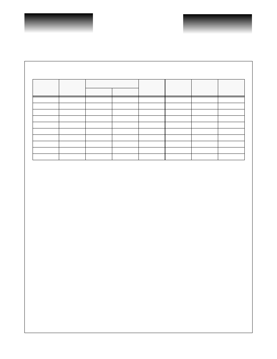
Part Number
Data Rate
(Gb/s)
Bandwidth
(MHz)
Input Noise
(
µ
W rms)
Optically Active Area
(
µ
m diameter)
VSC7710
1.25
1300
.22
75
∑ Integrated Photodetector/Transimpedance Ampli-
fier Family Optimized for High Speed Optical
Communications Applications
∑ Integrated AGC
∑ Fibre Channel and Gigabit Ethernet
∑ High Bandwidth
∑ Low Input Noise Equivalent Power
∑ Single 5V Supply
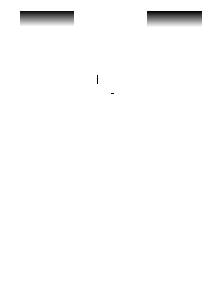
D0
D1
+5V
+
_

VITESSE
SEMICONDUCTOR CORPORATION
Advance Product Information
VSC7710
Photodetector/Transimpedance Amplifier
Family for Optical Communication
Page 2
G52139-0, Rev 2.2
04/02/01
© VITESSE
SEMICONDUCTOR CORPORATION ∑ 741 Calle Plano ∑ Camarillo, CA 93012
Tel: (800) VITESSE ∑ FAX: (805) 987-5896 ∑ Email: prodinfo@vitesse.com
Internet: www.vitesse.com
Table 1: Electro-Optic Specifications
Symbol
Parameter
Min
Typ
Max
Units
Conditions
V
DD
Supply Voltage
4.5
5.5
V
Wavelength
1270
1355
nm
f
c
Low Frequency Cutoff
1.4
MHz
-3dB
P = -22dBm, f
r
= 50MHz
T
r
T
f
Rise/Fall Time
300
ps
20% to 80%
P = -3 dBm
S
Sensitivity
-28
dBm
BER 10
-12
B = 1063Mb/s
D
r
Dynamic Range
25
dB
R
o
Single Ended Output Impedance
25
90
æ
V
d
Differential Output Voltage
0.25
1.2
V
P = -3 dBm, R = 100
PSRR
Power Supply Rejection Ratio
35
dB
f = 0.3MHz - 40MHz
Hybrid Differential
I
s
Supply Current
62
mA
P = -28 to -3 dBm
BW
Optical Modulation Bandwidth
700
1300
MHz
-3dB
P = -22dBm, f
r
= 50MHz
Rd
Differential Responsivity
2.5
mV/µW
= 100
P = -22dBm f
r
= 50MHz
V
n
Output Noise Voltage
1.2
mV
RMS
BW = 1500MHz, P = 0mW
NEP
O
Input Noise Equivalent Optical Power
0.22
µW RMS
BW = 1500MHz, P = 0mW
PDJ
Pattern Dependent Jitter
60
ps
P = -3dBm
±10% Voltage Window
DCD
Duty Cycle Distortion
5
%
P = -3dBm
˝V
Bias Offset Voltage
200
mV
P = -3dBm

VITESSE
SEMICONDUCTOR CORPORATION
Advance Product Information
VSC7710
Photodetector/Transimpedance Amplifier
Family for Optical Communication
G52139-0, Rev 2.2
Page 3
04/02/01
© VITESSE
SEMICONDUCTOR CORPORATION ∑ 741 Calle Plano ∑ Camarillo, CA 93012
Tel: (800) VITESSE ∑ FAX: (805) 987-5896 ∑ Email: prodinfo@vitesse.com
Internet: www.vitesse.com
Figure 1: Amplitude vs. Frequency
Table 2: Absolute Maximum Ratings
Table 3: Recommended Operating Conditions
Symbol
Parameter
Limits
V
DD
Power Supply
6V
T
stg
Storage Temperature
-55∞C to 125∞C (case temperature under bias)
P
inc
Incident Optical Power
+3 dBm
Symbol
Parameter
Limits
V
DD
Power Supply
4.5-5.5V (5.0V nominal)
T
op
Operating Temperature
0∞C (ambient) to 70∞C case
Frequency response of VSC7710WB (Upper 3db frequency is measured with respect to response at 50 MHz)

VITESSE
SEMICONDUCTOR CORPORATION
Advance Product Information
VSC7710
Photodetector/Transimpedance Amplifier
Family for Optical Communication
Page 4
G52139-0, Rev 2.2
04/02/01
© VITESSE
SEMICONDUCTOR CORPORATION ∑ 741 Calle Plano ∑ Camarillo, CA 93012
Tel: (800) VITESSE ∑ FAX: (805) 987-5896 ∑ Email: prodinfo@vitesse.com
Internet: www.vitesse.com
Table 4: Pin Table Specifications for TO-46(ball lens), TO-56 (flat window) Packages and Bare Die
Note: Pin Diagram is identical for both TO-46 and TO-56 package styles.
Figure 2: Pin Diagram
Figure 3: Schematic View of Bare Die Pad Assignments
Symbol
Description
D
+
OUT
Data output normal (with reference to incident light)
D
≠
OUT
Data output complement (inverting) (with reference to incident light)
VDD
Power supply
GND
Ground (package case)
D+
OUT
D≠
OUT
GND
VDD
GND
GND
ANODE
ANODE
CATHODE
D+
OUT
D≠
OUT
VDD
VDD

VITESSE
SEMICONDUCTOR CORPORATION
Advance Product Information
VSC7710
Photodetector/Transimpedance Amplifier
Family for Optical Communication
G52139-0, Rev 2.2
Page 5
04/02/01
© VITESSE
SEMICONDUCTOR CORPORATION ∑ 741 Calle Plano ∑ Camarillo, CA 93012
Tel: (800) VITESSE ∑ FAX: (805) 987-5896 ∑ Email: prodinfo@vitesse.com
Internet: www.vitesse.com
Thermal Resistance Calculation
In order to relate the junction temperature to an equivalent case temperature, the following thermal charac-
teristics of the package are provided (note that the thermal conductivity is identical for TO-46 and TO-56 pack-
age styles).
Table 5: Thermal Resistance Calculation for TO-56 and TO-46 Packages.
Chip Size
0.168cm x 0.104cm
Thermal Path
Chip Area A
0.015 cm
2
Die height (T
die
)
0.066 cm
Epoxy thickness (T
epoxy
)
0.0076 cm
Header thickness (Theader)
(ave. for TO-46 and TO-56)
0.115 cm
Thermal Conductivities
K GaAs
0.55W / cm ∞C
K epoxy
0.0186W / cm ∞C
K kovar
0.17W / cm ∞C
GaAs
K
GaAs
A
T
die
0.066
0.55 x 0.015
= 8
∞
C/W
=
=
epoxy
K
epoxy
A
T
epoxy
0.0076
0.0186 x 0.015
= 27.24
∞
C/W
=
=
kovar
K
kovar
A
T
kovar
0.12
0.17 x 0.015
= 47
∞
C/W
=
=
JC
= Thermal Resistance from Junction to Case = (8 + 27.24 + 47) = 82.24
∞
C/W
Example:
For VSC7710 at nominal supply current of 25mA and V
DD
= 5V
Temperature rise from junction to case = 0.025A x 5V x 82.24
∞
C/W = 10.28
∞
C
T
J
GaAs
EXPOXY
KOVAR
T
C

VITESSE
SEMICONDUCTOR CORPORATION
Advance Product Information
VSC7710
Photodetector/Transimpedance Amplifier
Family for Optical Communication
Page 6
G52139-0, Rev 2.2
04/02/01
© VITESSE
SEMICONDUCTOR CORPORATION ∑ 741 Calle Plano ∑ Camarillo, CA 93012
Tel: (800) VITESSE ∑ FAX: (805) 987-5896 ∑ Email: prodinfo@vitesse.com
Internet: www.vitesse.com
Figure 4: Eye Diagram

VITESSE
SEMICONDUCTOR CORPORATION
Advance Product Information
VSC7710
Photodetector/Transimpedance Amplifier
Family for Optical Communication
G52139-0, Rev 2.2
Page 7
04/02/01
© VITESSE
SEMICONDUCTOR CORPORATION ∑ 741 Calle Plano ∑ Camarillo, CA 93012
Tel: (800) VITESSE ∑ FAX: (805) 987-5896 ∑ Email: prodinfo@vitesse.com
Internet: www.vitesse.com
Notes on Measurement Conditions and Applications
Note 1: Noise Measurement Method
The noise voltage, Vn, at the output is referred back to the noise power at the input through the respon-
sivity R (with R in volts/watts)
The bit error rate can be expressed as:
For a
the parameter Q = 7
The sensitivity(s) at a bit error rate of
is calculated as follows:
where the NEP is in units of milliwatts and S is in dBm, respectively.
DUT
Board
P
2
3GHz BW
Hybrid Coupler
HP 437B
with
8481D
Power Sensor
Power Meter
RMS
Output
Noise
P
1
The noise voltage, (Vn), is calculated from the Output Noise Power, (Pn), into 50 ohm.
Vn
Pn
50
∑
=
NEP
Vn
R
-------
=
BER
1
12
≠
◊
10
=
1
12
≠
◊
10
(
Q
)
S = 10 log
10
NEP
1mW
,
e
(-Q
2
/
2
)
2
Q
BER
=

VITESSE
SEMICONDUCTOR CORPORATION
Advance Product Information
VSC7710
Photodetector/Transimpedance Amplifier
Family for Optical Communication
Page 8
G52139-0, Rev 2.2
04/02/01
© VITESSE
SEMICONDUCTOR CORPORATION ∑ 741 Calle Plano ∑ Camarillo, CA 93012
Tel: (800) VITESSE ∑ FAX: (805) 987-5896 ∑ Email: prodinfo@vitesse.com
Internet: www.vitesse.com
Note 2:Measurement Setup for Frequency Response
Note 3:Bias T Schematic
DC
1
AC
1
AC
2
DC
2
DUT
Hybrid
Coupler
Optical
Attenuator
Laser
Lightwave Component
Analyzer HP8702
Bias T
Bias T
Power
Supply
AC Out
DC Out
Signal

VITESSE
SEMICONDUCTOR CORPORATION
Advance Product Information
VSC7710
Photodetector/Transimpedance Amplifier
Family for Optical Communication
G52139-0, Rev 2.2
Page 9
04/02/01
© VITESSE
SEMICONDUCTOR CORPORATION ∑ 741 Calle Plano ∑ Camarillo, CA 93012
Tel: (800) VITESSE ∑ FAX: (805) 987-5896 ∑ Email: prodinfo@vitesse.com
Internet: www.vitesse.com
Package Information
Hybrid Die
VITESSE
SEMICONDUCTOR CORPORATION
Advance Product Information
VSC7710
Photodetector/Transimpedance Amplifier
Family for Optical Communication
Page 10
G52139-0, Rev 2.2
04/02/01
© VITESSE
SEMICONDUCTOR CORPORATION ∑ 741 Calle Plano ∑ Camarillo, CA 93012
Tel: (800) VITESSE ∑ FAX: (805) 987-5896 ∑ Email: prodinfo@vitesse.com
Internet: www.vitesse.com
Table 6: Die Pad Descriptions
Pad
Number
Pad
Name
Pad Locations
Pad
Size
Pass
Opening
Pad
Finish
Finish
Thickness
X
Y
1
ANODE
104.5
880
110 x 110
89 x 89
Gold
1500
≈
2
CLON
71.7
1440.6
110 x 110
89 x 89
Gold
1500
≈
3
VDD
71.7
1601.2
110 x 110
89 x 89
Gold
1500
≈
4
VGND
790
1602.1
110 x 110
89 x 89
Gold
1500
≈
5
CLOP
790
1441.1
110 x 110
89 x 89
Gold
1500
≈
6
ANODE
765.9
781.2
110 x 110
89 x 89
Gold
1500
≈
7
CATHODE
764.3
595.8
110 x 201
89 x 180
Gold
1500
≈
8
VGND
595.4
55
246 x 110
223 x 86
Gold
1500
≈
9
VDD
258
55
246 x 110
223 x 86
Gold
1500
≈
10
CATHODE
428.5
530.5
522 x 522
310 x 310
Gold
1500
≈

VITESSE
SEMICONDUCTOR CORPORATION
Advance Product Information
VSC7710
Photodetector/Transimpedance Amplifier
Family for Optical Communication
G52139-0, Rev 2.2
Page 11
04/02/01
© VITESSE
SEMICONDUCTOR CORPORATION ∑ 741 Calle Plano ∑ Camarillo, CA 93012
Tel: (800) VITESSE ∑ FAX: (805) 987-5896 ∑ Email: prodinfo@vitesse.com
Internet: www.vitesse.com
To-56 Flat Window
Reference Isometric

VITESSE
SEMICONDUCTOR CORPORATION
Advance Product Information
VSC7710
Photodetector/Transimpedance Amplifier
Family for Optical Communication
Page 12
G52139-0, Rev 2.2
04/02/01
© VITESSE
SEMICONDUCTOR CORPORATION ∑ 741 Calle Plano ∑ Camarillo, CA 93012
Tel: (800) VITESSE ∑ FAX: (805) 987-5896 ∑ Email: prodinfo@vitesse.com
Internet: www.vitesse.com
To-46 Ball Lens--7mm Lead Length
Reference Isometric

VITESSE
SEMICONDUCTOR CORPORATION
Advance Product Information
VSC7710
Photodetector/Transimpedance Amplifier
Family for Optical Communication
G52139-0, Rev 2.2
Page 13
04/02/01
© VITESSE
SEMICONDUCTOR CORPORATION ∑ 741 Calle Plano ∑ Camarillo, CA 93012
Tel: (800) VITESSE ∑ FAX: (805) 987-5896 ∑ Email: prodinfo@vitesse.com
Internet: www.vitesse.com
TO-46 Ball Lens--13mm Lead Length
Reference Isometric
VITESSE
SEMICONDUCTOR CORPORATION
Advance Product Information
VSC7710
Photodetector/Transimpedance Amplifier
Family for Optical Communication
Page 14
G52139-0, Rev 2.2
04/02/01
© VITESSE
SEMICONDUCTOR CORPORATION ∑ 741 Calle Plano ∑ Camarillo, CA 93012
Tel: (800) VITESSE ∑ FAX: (805) 987-5896 ∑ Email: prodinfo@vitesse.com
Internet: www.vitesse.com
Ordering Information
The order number for this product is formed by a combination of the device type and package type.
Notice
Vitesse Semiconductor Corporation ("Vitesse") provides this document for informational purposes only. This document contains pre-production
information about Vitesse products in their concept, development and/or testing phase. All informaiton in this document, including descriptions of
features, functions, performance, technical specifications and availability, is subject to change without notice at any time. Nothing contained in this
document shall be construed as extending any warranty or promise, express or implied, that any Vitesse product will be available as described or
will be suitable for or will accomplish any particular task.
Vitesse products are not intended for use in life support appliances, devices or systems. Use of a Vitesse product in such applications without writ-
ten consent is prohibited.
VSC7710 xx
Device Type
Package
Photodetector/Transimpedance Amplifier
Family for Optical Communication
WB: TO-56 Flat Window
WC: TO-46 Ball Lens--7mm Lead Length
WD: TO-46 Ball Lens--13mm Lead Length
X:
Bare Dice