 | –≠–ª–µ–∫—Ç—Ä–æ–Ω–Ω—ã–π –∫–æ–º–ø–æ–Ω–µ–Ω—Ç: VSC8115YA | –°–∫–∞—á–∞—Ç—å:  PDF PDF  ZIP ZIP |

©
VITESSE
SEMICONDUCTOR CORPORATION
Page 1
9/29/00
741 Calle Plano, Camarillo, CA 93012 ∑ 805/388-3700 ∑ FAX: 805/987-5896
VITESSE
SEMICONDUCTOR CORPORATION
Target Specification
VSC8115
STS-12/STS-3 Multi Rate
Clock and Data Recovery Unit
G52272-0, Rev. 1.1
Features
General Description
The VSC8115 functions as a clock and data recovery unit for SONET/SDH-based equipment to derive high
speed timing signals. The VSC8115 recovers the clock from the scrambled NRZ data operating at 622.08Mb/s
(STS-12/OC-12/STM-4) or 155.52Mb/s (STS-3/OC-3/STM-1). After the clock is recovered, the data is retimed
using an output flip-flop. Both recovered clock and retimed data outputs can be configured as LVDS or
LVPECL signals to facilitate a low-jitter and low power interface.
VSC8115 Block Diagram
∑ Performs clock and data recovery for
622.08Mb/s (STS-12/OC-12/STM-4) or
155.52Mb/s (STS-3/OC-3/STM-1) NRZ data
∑ Meets Bellcore, ITU and ANSI Specifications
for Jitter Performance
∑ 19.44MHz reference frequency LVTTL Input
∑ Lock Detect output pin monitors data run length
and frequency drift from the reference clock
∑ Data is Retimed at the Output
∑ Active High Signal Detect LVPECL Input
∑ Low-jitter high speed outputs can be configured
as either LVPECL or low power LVDS
∑ Low power - 0.188 Watts Typical Power
∑ +3.3V Power Supply
∑ 20 Pin TSSOP Package
∑ Requires One External Capacitor
∑ PLL bypass operation facilitates the board
debug process
1
0
2
2
CLKOUT+/-±
LOCKDET
DATAOUT+/-
LOCKREFN
DATAIN+/-
SD
REFCLK
STS12
Phase/
Loop Filter
Divider
Freq
Detector
VCO
CAP+
CAP-
BYPASS
2

VITESSE
SEMICONDUCTOR CORPORATION
Target Specification
VSC8115
STS-12/STS-3 Multi Rate
Clock and Data Recovery Unit
Page 2
©
VITESSE
SEMICONDUCTOR CORPORATION
741 Calle Plano, Camarillo, CA 93012 ∑ 805/388-3700 ∑ FAX: 805/987-5896
9/29/00
G52272-0, Rev. 1.1
Functional Description
The VSC8115 contains an on-chip PLL consisting of a phase/frequency detector, a loop filter using one
external capacitor, a LC-based voltage-controlled oscillator (VCO), and a programmable frequency divider.
The phase/frequency detector compares the phase relationship between the VCO output and an external
19.44MHz LVTTL reference clock to make coarse adjustment to the VCO block so that its output is held within
+500ppm of the reference clock. The use of reference clock minimizes the PLL lock time during power up and
provides a stable output clock source in the absence of serial input data. The phase/frequency detector also com-
pares the phase relationship between the VCO output and the serial data input to make fine adjustment to the
VCO block. The loop filter converts the phase detector output into a smooth DC voltage. This DC voltage is
used as the input to the VCO block whose output frequency is a function of the input voltage. A programmable
frequency divider down converts the VCO output signal and provides two modes of operation: 622.08Mb/s
mode if STS12 is HIGH, or 155.52Mb/s mode if STS12 is LOW.
Lock Detection
The VSC8115 features a lock detection for the PLL. The lock detect (LOCKDET) output goes HIGH to
indicate that the PLL is locked to the serial data inputs and that valid data and clock are present at the high speed
differential outputs. If LOCKDET output is LOW, then either the PLL is forced to lock to the REFCLK input or
the VCO has drifted away from the local reference clock by more than 500 ppm.
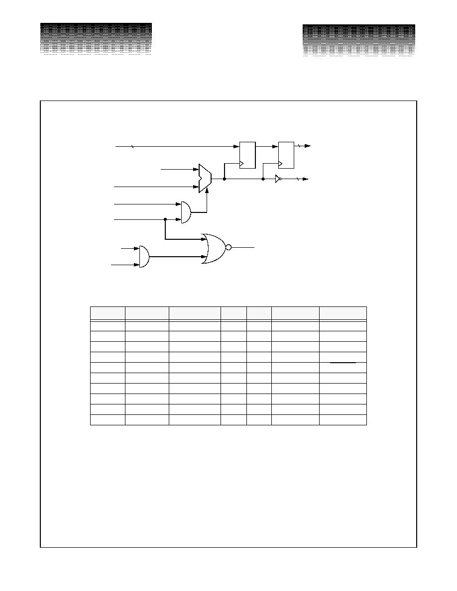
Signal Detection
The VSC8115 has a signal detect (SD) input and a lock-to-reference (LOCKREFN) input. The SD pin is a
LVPECL input, and the LOCKREFN pin is a LVTTL input. These two control pins are used to indicate a loss
of signal condition and they are connected inside the part as shown in Figure 1. If either one of these two inputs
goes LOW and BYPASS is LOW, the VSC8115 will enter the loss of signal (LOS) state, and it will hold the
DATAOUT+/- output at logic LOW state. During the LOS state, the VSC8115 also will hold the output clock
CLKOUT+/- to within +500ppm of the REFCLK. See Table 1.
Most of the optical module has a signal detect output. This signal detect output indicates that there is suffi-
cient optical power, and it is typically active HIGH. If the signal detect output on the optical module is
LVPECL, it should be connected directly to the SD input on the VSC8115, and the LOCKREFN input needs to
be tied HIGH. If the signal detect output is LVTTL, it should be connected directly to the LOCKREFN input,
and the SD input needs to be tied HIGH.
The SD and LOCKREFN inputs also can be used for other applications when the users need to hold the
CLKOUT+/- output to within +500ppm of the reference clock and to force the DATAOUT+/- output to the
logic LOW state.
PLL Bypass Operation
The BYPASS pin is intended for use in production test, and it should be set at logic LOW in the normal
operation. If both BYPASS and MODE pins are set at logic HIGH, the VSC8115 will bypass the PLL and will
present an inverted version of the REFCLK to the clock output CLKOUT+/-. The REFCLK's rising edge is
used to capture data at DATAIN+/- and transmit data at DATAOUT+/-. This bypass operation can be used to
facilitate the board debug process.
©
VITESSE
SEMICONDUCTOR CORPORATION
Page 3
9/29/00
741 Calle Plano, Camarillo, CA 93012 ∑ 805/388-3700 ∑ FAX: 805/987-5896
VITESSE
SEMICONDUCTOR CORPORATION
Target Specification
VSC8115
STS-12/STS-3 Multi Rate
Clock and Data Recovery Unit
G52272-0, Rev. 1.1
Figure 1: Control Diagram for Signal Detection and PLL Bypass Operation
Table 1: Signal Detection and PLL Bypass Operation Control
STS12
BYPASS
LOCKREFN
SD
LOS
DATAOUT
CLKOUT
1
0
1
1
0
DATIN
PLL Clock
1
0
1
0
1
LOW
PLL Clock
1
0
0
1
1
LOW
PLL Clock
1
0
0
0
1
LOW
PLL Clock
1
1
X
X
0
DATIN
REFCLK
0
0
1
1
0
DATIN
PLL Clock
0
0
1
0
1
LOW
PLL Clock
0
0
0
1
1
LOW
PLL Clock
0
0
0
0
1
LOW
PLL Clock
0
1
X
X
0
Not Allowed
Not Allowed
1
0
2
CLKOUT+/-±
DATAOUT+/-
BYPASS
DATAIN+/-
STS12
REFCLK
2
PLL Clock
(on-chip)
2
LOCKREFN
SD
LOS
(on-chip)

VITESSE
SEMICONDUCTOR CORPORATION
Target Specification
VSC8115
STS-12/STS-3 Multi Rate
Clock and Data Recovery Unit
Page 4
©
VITESSE
SEMICONDUCTOR CORPORATION
741 Calle Plano, Camarillo, CA 93012 ∑ 805/388-3700 ∑ FAX: 805/987-5896
9/29/00
G52272-0, Rev. 1.1
AC Characteristics
Table 2: Performance Specifications
Parameters
Min
Typ
Max
Units
Conditions
VCO Center Frequency
--
622.08
--
MHz
CRU's Reference Clock Frequency
Tolerance
-250
--
+250
ppm
OC-12/STS12 Capture Range
--
--
ppm
With respect to the fixed
reference frequency
Clock Output Duty Cycle
45
--
55
% of UI
20% Minimum transition
density
Acquisition Lock Time OC-12/STS-12
--
--
16
µ
s
Valid REFCLK and device
already powered up
LVDS Output Rise & Fall Times
--
--
600
ps
10% to 90%, with 100
& 5pF
capacitive equivalent load
CLKOUT+/- Jitter Generation
--
0.005
0.01
U.I.
No more than 14ps rms jitter on
DATAIN+/-
OC-12/STS-12 Jitter Tolerance
0.5
--
--
U.I.
Sinusoidal input jitter of
DATAIN+/- from 250KHz to
5MHz
500
±
©
VITESSE
SEMICONDUCTOR CORPORATION
Page 5
9/29/00
741 Calle Plano, Camarillo, CA 93012 ∑ 805/388-3700 ∑ FAX: 805/987-5896
VITESSE
SEMICONDUCTOR CORPORATION
Target Specification
VSC8115
STS-12/STS-3 Multi Rate
Clock and Data Recovery Unit
G52272-0, Rev. 1.1
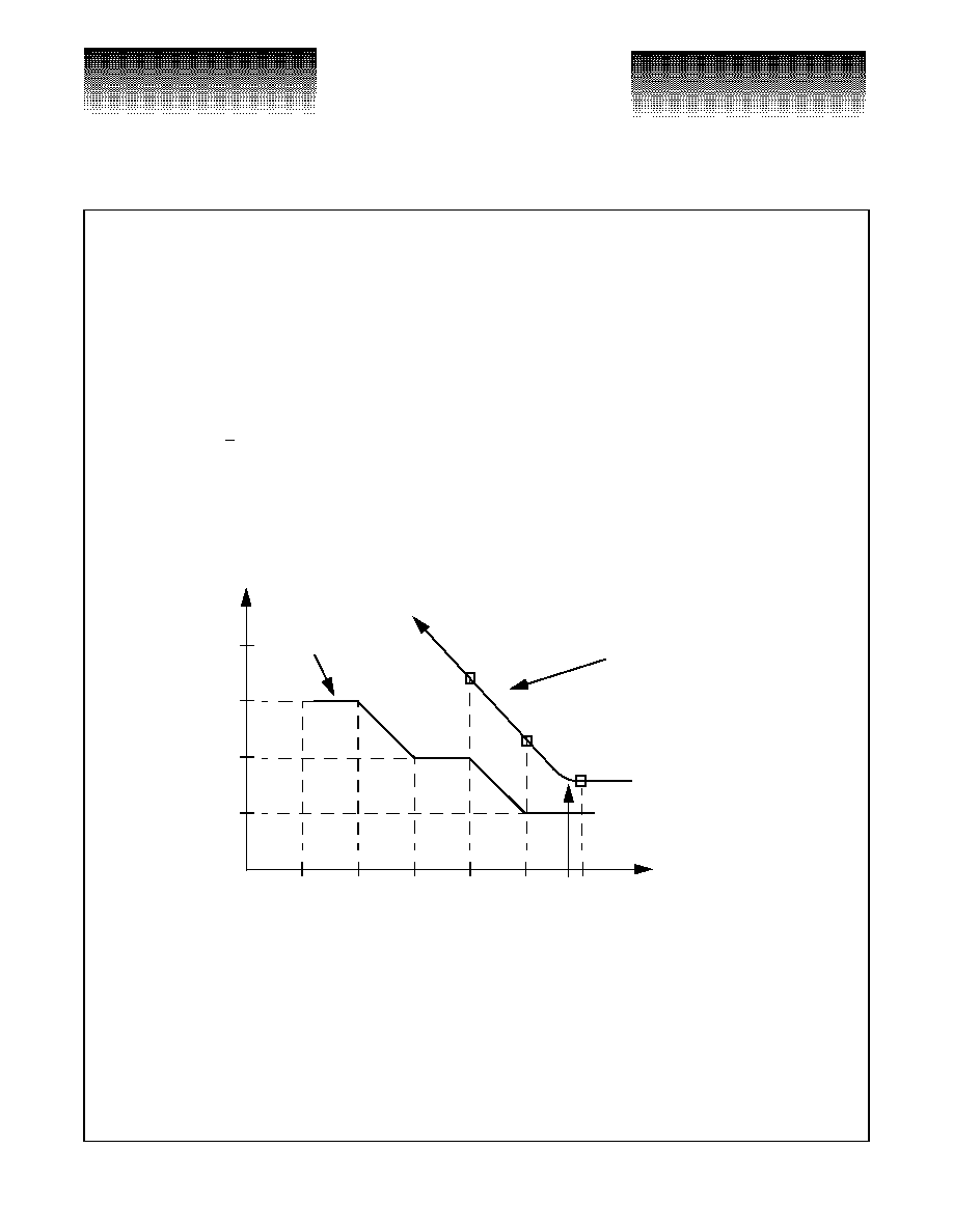
Jitter Tolerance
Jitter Tolerance is the ability of the Clock and Data Recovery Unit to track timing variation in the received
data stream. The Bellcore and ITU specifications allow the received optical data to contain jitter. The amount
that must be tolerated is a function of the frequency of the jitter. At high frequencies the specifications do not
require the VSC8115 to tolerate large amounts, whereas at low frequencies many unit intervals (bit times) of jit-
ter have to be tolerated. Jitter tolerance is defined as the ratio of jitter on the output OC-N/STS-N signal to the
jitter applied on the input OC-N/STSN signal versus frequency. The VSC8115 is designed to tolerate this jitter
with margin over the specification limits, see Figure 2. The VSC8115 obtains and maintains lock based on the
data transition information. When there is no transition on the data stream, the recovered clock frequency will
be held to within +500ppm of the reference clock. The VSC8115 can maintain lock over 1000 bits of no switch-
ing on data stream.
Figure 2: Input Jitter Tolerance Specification
Jitter Generation
Jitter generation is defined as the jitter of the serial clock and serial data outputs while rms jitter is presented
to the serial data inputs. Maximum jitter generation is 0.01 U.I. when rms jitter of less than 14ps (OC-12) or
56ps (OC-3) is presented to the serial data inputs.
10
30
300
25K
250K
15
1.5
0.15
J
ITTER
F
REQ
(H
Z
)
J
ITTER
(UI
P
-
P
)
2.5M
150
24
2.4
0.6
Bellcore Requirement
VSC8115 Typical
Jitter Tolerance
1M