 | –≠–ª–µ–∫—Ç—Ä–æ–Ω–Ω—ã–π –∫–æ–º–ø–æ–Ω–µ–Ω—Ç: VSC8140 | –°–∫–∞—á–∞—Ç—å:  PDF PDF  ZIP ZIP |

©
VITESSE
SEMICONDUCTOR CORPORATION
Page 1
9/6/00
741 Calle Plano, Camarillo, CA 93012 ∑ 805/388-3700 ∑ FAX: 805/987-5896
VITESSE
SEMICONDUCTOR CORPORATION
Data Sheet
VSC8140
2.48832Gb/s 16:1 SONET/SDH
Transceiver with Integrated Clock Generator
G52251-0, Rev. 4.0
Features
General Description
The VSC8140 is a SONET/SDH compatible transceiver with integrated clock generator for use in SONET/
SDH systems operating at a 2.48832Gb/s data rate. The internal clock generator uses a Phase-Locked Loop
(PLL) to multiply either a 77.76MHz or 155.52MHz reference clock in order to provide the 2.48832GHz clock
for internal logic and output retiming. The 16-bit parallel interface incorporates an on-board FIFO eliminating
loop timing design issues by providing a flexible parallel timing architecture. In addition, the device provides
both facility and equipment loopback modes and two loop timing modes. The VSC8140 operates using a 3.3V
power supply, and is available in either a thermally-enhanced 128-PQFP or a thermally-enhanced 208-pin
TBGA package.
VSC8140 Block Diagram
∑ 2.48832Gb/s 16-Bit Transceiver
∑ Targeted for SONET OC-48 / SDH STM-16
Applications
∑ LVPECL Low-Speed Interface
∑ On-chip PLL-Based Clock Generator
∑ High-Speed Clock Output With Power-Down
Option
∑ Supports Parity at the 16-Bit Parallel Transmit
and Receive Interfaces
∑ Provides Equipment, Facilities and Split Loop-
back Modes as well as Loop Timing Modes
∑ Loss of Signal (LOS) Detect input
∑ Meets Bellcore Jitter Performance Specifications
∑ Single +3.3V Supply
∑ 2.25 Watts Typical Power Dissipation
∑ Packages: 128-pin PQFP or 208-pin TBGA
RXOUT15
TXIN15
RXOUT0
RXPARITYOUT
RXCLK16O+
RXCLK16O-
RXCLKIN+
RXCLKIN-
O
u
t
p
u
t
R
e
gi
st
er
RXCLKO16_32+
RXCLKO16_32-
Divide by
2
TXIN0
TXPARITYIN
TXCLK16O+
TXCLK16O-
TXOUT+
TXOUT-
I
npu
t R
e
gi
st
er
Divide by
16
REFCLK+
REFCLK-
2.48832GHz
PLL
TXCLK16I+
TXCLK16I-
Q D
FACLOOP
LOOPTIM0
FIFO
CNTRL
FIFORESET
Divide by
16
EQULOOP
D Q
RXIN+
RXIN-
TXCLKOUT+
TXCLKOUT-
LPTIMCLK+
LPTIMCLK-
Write
Pointer
Read
Pointer
1
6x5 FI
FO
PARERR
LOS
POL
OVERFLOW
VREFOUT
voltage
gen.
REF_FREQSEL
LOOPTIM1
PARMODE
RXCLKO_FREQSEL
VREFIN
CLK128O+
CLK128O-
Divide
by 128

VITESSE
SEMICONDUCTOR CORPORATION
Data Sheet
VSC8140
2.48832Gb/s 16:1 SONET/SDH
Transceiver with Integrated Clock Generator
Page 2
©
VITESSE
SEMICONDUCTOR CORPORATION
741 Calle Plano, Camarillo, CA 93012 ∑ 805/388-3700 ∑ FAX: 805/987-5896
9/6/00
G52251-0, Rev. 4.0
Functional Description
Transmitter Low-Speed Interface
The Upstream Device should use the TXCLK16O as the timing source for its final output latch (see Figure
1). The Upstream Device should then generate a TXCLK16I that is phase-aligned with the data. The VSC8140
will latch TXIN[15:0]
±
on the rising edge of TXCLK16I+. The data must meet setup and hold times with
respect to TXCLK16I (see Table 1).
A FIFO exists within the VSC8140 to eliminate difficult system loop timing issues. Once the PLL has
locked to the reference clock, RESET must be held low for a minimum of five CLK16 cycles to initialize the
FIFO, then RESET should be set high and held constant for continuous FIFO operation. For the transparent
mode of operation (no FIFO), simply hold RESET at a constant low state (see Figure 2).
The use of a FIFO permits the system designer to tolerate an arbitrary amount of delay between
TXCLK16O and TXCLK16I. Once RESET is asserted and the FIFO initialized, the delay between TXCLK16O
and TXCLK16I can decrease or increase up to one period of the low-speed clock (6.4ns). Should this delay drift
exceed one period, the write pointer and the read pointer could point to the same word in the FIFO, resulting in
a loss of transmitted data (a FIFO overflow). In the event of a FIFO overflow, an active low OVERFLOW sig-
nal is asserted (for a minimum of five TXCLK16I cycles) which can be used to initiate a reset signal from an
external controller.
The TXCLK16O
±
output driver is a LVPECL output driver designed to drive a 50
transmission line. The
transmission line can be DC terminated with a split-end termination scheme (see Figure 3), or DC terminated by
50
to V
CC
-2V on each line (see Figure 4). At any time, the equivalent split-end termination technique can be
substituted for the traditional 50
to V
CC
-2V on each line. AC-coupling can be achieved by a number of meth-
ods. Figure 5 illustrates an AC-coupling method for the occasion when the downstream device provides the bias
point for AC-coupling.
Figure 1: Low-Speed Systems Interface
write
16
read
16 x 5 FIFO
VSC8140
2.48832GHz
PLL
REFCLK
Div 16
TXCLK16I
TXCLK16O
OVERFLOW

©
VITESSE
SEMICONDUCTOR CORPORATION
Page 3
9/6/00
741 Calle Plano, Camarillo, CA 93012 ∑ 805/388-3700 ∑ FAX: 805/987-5896
VITESSE
SEMICONDUCTOR CORPORATION
Data Sheet
VSC8140
2.48832Gb/s 16:1 SONET/SDH
Transceiver with Integrated Clock Generator
G52251-0, Rev. 4.0
Figure 2: Enabling FIFO Operation
Figure 3: DC Termination of Low-Speed LVPECL RXCLK16O, RXCLK16_32O, TXCLK16O Outputs
Figure 4: DC Termination of Low-Speed LVPECL RXCLK16O, RXCLK16_32O, TXCLK16O Outputs
Minimum 5 CLK16 cycles
FIFO Mode Operation
Transparent Mode Operation
Holding RESET "low" for a minimum of 5 CLK16 cycles, then setting "high" enables FIFO operation.
Holding RESET constantly "low" bypasses the FIFO for transparent mode operation.
PLL locked to reference clock.
RESET
VSC8140
Z
o
R2
R2
R1
R1
V
EE
V
CC
V
CC
R2 + V
EE
R1
R1+R2
= V
TERM
downstream
R1||R2 = Z
O
Z
o
Split-end equivalent termination is Z
O
to V
TERM
R1 = 125
R2 = 83
, Z
O
=50
, V
TERM
= V
CC
-2V
V
CC
-2V
R1 =50
VSC8140
Z
o
V
CC
-2V
R1 =50
downstream

VITESSE
SEMICONDUCTOR CORPORATION
Data Sheet
VSC8140
2.48832Gb/s 16:1 SONET/SDH
Transceiver with Integrated Clock Generator
Page 4
©
VITESSE
SEMICONDUCTOR CORPORATION
741 Calle Plano, Camarillo, CA 93012 ∑ 805/388-3700 ∑ FAX: 805/987-5896
9/6/00
G52251-0, Rev. 4.0
Figure 5: AC Termination of Low-Speed LVPECL RXCLK16O, RXCLK16_32O, TXCLK16O Outputs
Receiver Low-Speed Interface
The demultiplexed serial stream is made available by a 16-bit single-ended LVPECL interface
RXOUT[15:0] with accompanying differential LVPECL divide-by-16 clock RXCLK16O
±
and selectable
LVPECL divide-by-16 or -32 clock RXCLK16_32O
±
.
RXCLKO_FREQSEL is used to select RXCLK16_32O
±
. RXCLKO_FREQSEL = "0" designates
RXCLK16_32O
±
output as 77.76MHz, RXCLKO_FREQSEL = "1" designates RXCLK16_32O
±
output as
155.52MHz.
The RXCLK16O and RXCLK16_32O output drivers are designed to drive a 50
transmission line. The
transmission line can be DC terminated with a split-end termination scheme (see Figure 3), or DC terminated by
50
to V
CC
-2V on each line (see Figure 4). AC-coupling can be achieved by a number of methods. Figure 5
illustrates an AC-coupling method for the occasion when the downstream device provides the bias point for
AC-coupling. The divide-by-16 output (RXCLK16O) or the divide-by-16 or -32 output (RXCLK16_32O) can
be used to provide an external looptiming reference clock (after external filtering with a 1x REFCLK PLL) for
the clock multiplication unit on the VSC8140.
The RXOUT[15:0] output drivers are designed to drive a 50
transmission line which can be DC termi-
nated with a split-end termination scheme (see Figure 6), or a traditional termination scheme (see Figure 7).
Figure 6: Split-end DC Termination of Low-Speed LVPECL RXOUT[15:0] Outputs
VSC8140
100nF
50
50
Z
o
Z
o
100nF
V
CC
-2V
downstream
bias point
generated
internally
VSC8140
Z
o
R1 = 125
V
EE
V
CC
R2 = 83
Split-end equivalent termination is Z
O
to V
TERM
R1 = 125
R2 = 83
, Z
O
=50
, V
TERM
= V
CC
-2V
V
CC
R2 + V
EE
R1
R1+R2
= V
TERM
R1||R2 = Z
o

©
VITESSE
SEMICONDUCTOR CORPORATION
Page 5
9/6/00
741 Calle Plano, Camarillo, CA 93012 ∑ 805/388-3700 ∑ FAX: 805/987-5896
VITESSE
SEMICONDUCTOR CORPORATION
Data Sheet
VSC8140
2.48832Gb/s 16:1 SONET/SDH
Transceiver with Integrated Clock Generator
G52251-0, Rev. 4.0
Figure 7: Traditional DC Termination of Low-Speed LVPECL RXOUT[15:0] Outputs
The RXOUT[15:0] output drivers can also be appropriately AC-coupled by a number of methods, how-
ever, DC-coupling is preferred since there is no guarantee of transition density for individual bits in the 16-bit
word. Figure 8 illustrates an AC-coupling method for the occasion when the downstream device provides the
bias point for AC-coupling. Figure 9 illustrates an AC-coupling method for the occasion when the bias point
needs to be generated externally. The resistor values in Figure 9 were selected to generate a bias point of 1.98V,
the mid-point for LVPECL V
OH
and V
OL
as specified for the VSC8140. Resistor values should be selected to
generate the necessary bias point for the downstream device.
Figure 8: AC Termination of Low-Speed LVPECL RXOUT[15:0] Outputs
VSC8140
Z
o
V
CC
-2V
R1 =50
VSC8140
Z
o
R1 = 50
V
CC
-2V
100nF
downstream
bias point
generated
internally

VITESSE
SEMICONDUCTOR CORPORATION
Data Sheet
VSC8140
2.48832Gb/s 16:1 SONET/SDH
Transceiver with Integrated Clock Generator
Page 6
©
VITESSE
SEMICONDUCTOR CORPORATION
741 Calle Plano, Camarillo, CA 93012 ∑ 805/388-3700 ∑ FAX: 805/987-5896
9/6/00
G52251-0, Rev. 4.0
Figure 9: AC Termination of Low-Speed LVPECL RXOUT[15:0] Outputs
Parity
Systems employing internal parity are supported by the VSC8140. On the transmit side, a parity check is
performed between the TXPARITYIN input and the 16 TXIN[15:0] bits.
PARMODE is used to select even or odd parity expected for these 17 bits. (TXIN[15:0] and TXPARI-
TYIN). PARMODE = "0" selects odd, PARMODE = "1" selects even. The PARERR output (parity error out-
put) is asserted active high when the parity of the 17 bits (TXIN[15:0] and TXPARITYIN) does not conform to
the expected parity designated by PARMODE. PARERR becomes available T
DV
after the rising edge of
TXCLK16I. PARERR is a NRZ pulse that is updated every 6.4 ns, i.e., the period of TXCLK16I. The timing
relationship of PARERR to TXCLK16I is shown in Figure 17. The PARERR pin may be left open if parity is
unused.
On the receive side, the parity output (RXPARITYOUT) is simply the XOR of all 16 outputs.
Loss of Signal
The VSC8140 has a TTL input LOS to force the part into a Loss of Signal (LOS) state. Most optics have a
TTL output usually called Signal Detect (SD), based on the optical power of the incoming light stream.
Depending on the optics manufacturer, this signal is either active high or low. To accommodate polarity differ-
ences, the internal Loss of Signal is generated when the POL and LOS inputs are of opposite states. Once active,
all zeroes "0" will be propagated downstream using the transmit clock until the optical signal is regained and
LOS and POL are in the same logic state.
VSC8140
Z
o
R3 =83
V
EE
V
CC
R4 = 125
100nF
R1 = 125
V
EE
V
CC
R2 = 83
downstream
bias point
generated
externally

©
VITESSE
SEMICONDUCTOR CORPORATION
Page 7
9/6/00
741 Calle Plano, Camarillo, CA 93012 ∑ 805/388-3700 ∑ FAX: 805/987-5896
VITESSE
SEMICONDUCTOR CORPORATION
Data Sheet
VSC8140
2.48832Gb/s 16:1 SONET/SDH
Transceiver with Integrated Clock Generator
G52251-0, Rev. 4.0
Figure 10: Facility Loopback Data Path
Facility Loopback
The facility loopback function is controlled by the FACLOOP signal. When the FACLOOP signal is set
high, the Facility Loopback mode is activated and the high-speed serial receive data (RXIN) is presented at the
high-speed transmit output (TXOUT), as depicted in Figure 10. In addition, the high-speed receive clock input
(RXCLKI) is selected and presented at the high-speed transmit clock output (TXCLKOUT). In Facility Loop-
back mode, the high-speed receive data (RXIN) is also converted to parallel data and presented at the low-speed
receive output pins (RXOUT[15:0]). The receive clock (RXCLKIN) is also divided down and presented at the
low-speed clock output (RXCLK16O).
Equipment Loopback Data Path
The Equipment Loopback function is controlled by the EQULOOP signal, which is active high. When the
Equipment Loopback mode is activated, the high-speed transmit data generated from the parallel to serial con-
version of the low-speed data (TXIN[15:0]) is selected and converted back to parallel data in the receiver sec-
tion and presented at the low-speed parallel data outputs (RXOUT[15:0]), as shown in Figure 11. The internally
generated OC-48 clock is used to generate the low-speed receive output clocks (RXCLK16O and
RXCLK16_32O). In Equipment Loopback mode, the transmit data (TXIN[15:0]) is serialized and presented at
the high-speed output (TXOUT) along with the high-speed transmit clock (TXCLKOUT) which is generated by
the on-chip PLL.
RXCLKIN+
RXCLKIN-
TXOUT+
TXOUT-
2.48832GHz
PLL
Q D
FACLOOP
D Q
RXIN+
RXIN-
TXCLKOUT+
TXCLKOUT-
1
0
1
0
16:1 Parallel to
Serial
1:16 Serial to
Parallel
RXOUT[15:0]
RXCLK16O
RXCLK32O

VITESSE
SEMICONDUCTOR CORPORATION
Data Sheet
VSC8140
2.48832Gb/s 16:1 SONET/SDH
Transceiver with Integrated Clock Generator
Page 8
©
VITESSE
SEMICONDUCTOR CORPORATION
741 Calle Plano, Camarillo, CA 93012 ∑ 805/388-3700 ∑ FAX: 805/987-5896
9/6/00
G52251-0, Rev. 4.0
Figure 11: Equipment Loopback Data Path
Figure 12: Split Loopback Datapaths
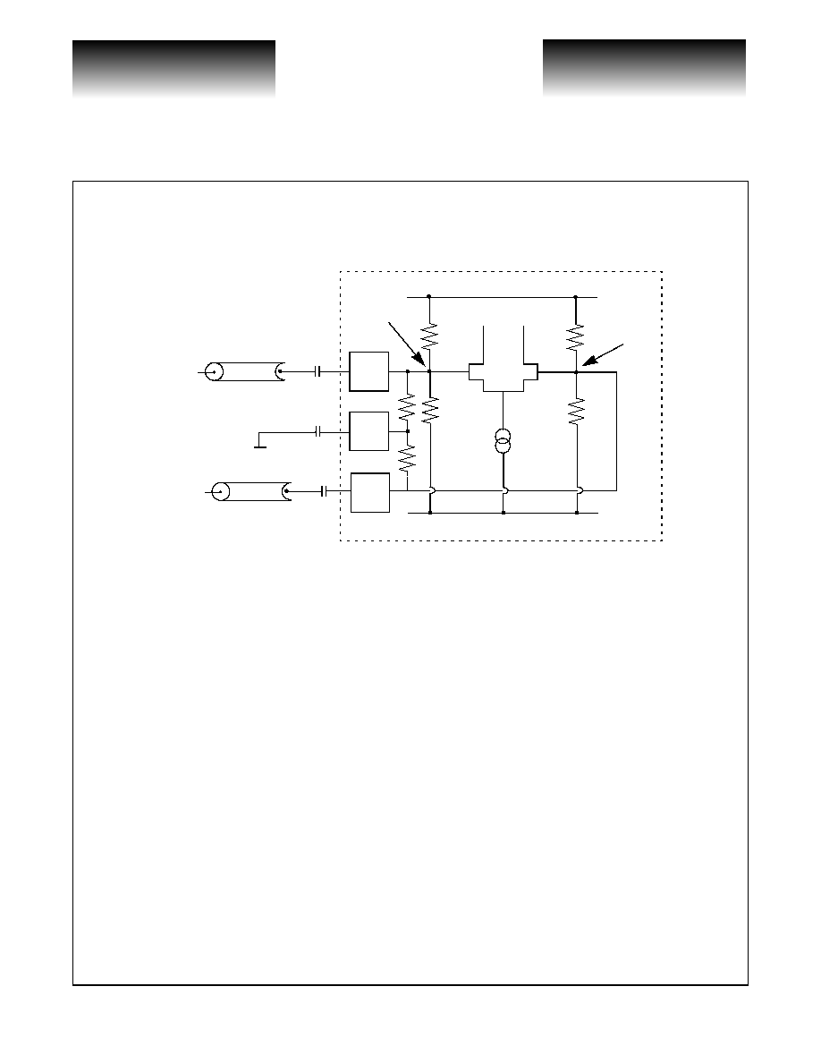
Split Loopback
Equipment and Facility Loopback modes can be enabled simultaneously. In this case, high-speed serial data
received (RXIN) and clock (RXCLKIN) are muxed through to the high-speed serial outputs (TXOUT and
TXCLKOUT). The low-speed 16-bit transmit stream (TXIN[15:0]) is muxed into the low-speed 16-bit receive
output stream (RXOUT[15:0]). See Figure 12.
Looptiming
LOOPTIM0 mode bypasses the PLL when LOOPTIM0 is asserted high. In this mode, the PLL is bypassed
using the receive high-speed clock (RXCLKIN), and the entire part is synchronously clocked from a single
external source.
RXCLK32O
RXCLKIN+
RXCLKIN-
TXOUT+
TXOUT-
Q D
EQULOOP
D Q
RXIN+
RXIN-
TXCLKOUT+
TXCLKOUT-
1
1
0
0
16:1 Parallel to
1:16 Serial to
Parallel
RXOUT[15:0]
RXCLK16O
TXCLK16O
TXIN[15:0]
TXCLK16I
Serial
2.48832GHz
PLL
RXCLK32O
EQULOOP
1
1
0
0
16:1 Parallel to
1:16 Serial to
Parallel
RXOUT[15:0]
RXCLK16O
TXCLK16O
TXIN[15:0]
TXCLK16I
2.48832GHz
PLL
RXCLKIN+
RXCLKIN-
TXOUT+
TXOUT-
Q D
FACLOOP
D Q
RXIN+
RXIN-
TXCLKOUT+
TXCLKOUT-
1
0
1
0
Serial
©
VITESSE
SEMICONDUCTOR CORPORATION
Page 9
9/6/00
741 Calle Plano, Camarillo, CA 93012 ∑ 805/388-3700 ∑ FAX: 805/987-5896
VITESSE
SEMICONDUCTOR CORPORATION
Data Sheet
VSC8140
2.48832Gb/s 16:1 SONET/SDH
Transceiver with Integrated Clock Generator
G52251-0, Rev. 4.0
When LOOPTIM1 is asserted high, the RXCLK16_32O or RXCLK16O output can be tied to the LPTIM-
CLK input. In order to meet jitter transfer, the RXCLK16_32O or RXCLOCK16O needs to be filtered by a 1X
PLL circuit with a narrow pass characteristic. The part is forced out of this mode in Equipment Loopback to
prevent the PLL from feeding its own clock back.
Clock Generator
An on-chip PLL generates the 2.48832GHz transmit clock from the externally provided REFCLK input.
The on-chip PLL uses a low phase noise reactance-based Voltage Controlled Oscillator (VCO) with an on-chip
loop filter (with two external 0.1
µ
F peaking capacitors). The loop bandwidth of the PLL is within the SONET
specified limit of 2MHz.
The customer can select to provide either a 77.76MHz reference, or 2x of that reference, 155.52MHz.
REF_FREQSEL is used to select the desired reference frequency. REF_FREQSEL = "0" designates REFCLK
input
as 77.76MHz, REF_FREQSEL = "1" designates REFCLK input as 155.52MHz.
The REFCLK should be of high quality since noise on the REFCLK below the loop bandwidth of the PLL
will pass through the PLL and appear as jitter on the output. Preconditioning of the REFCLK signal with a
VCXO may be required to avoid passing REFCLK noise with greater than 2ps RMS of jitter to the output. The
VSC8140 will output the REFCLK noise in addition to the intrinsic jitter from the VSC8140 itself during such
conditions.
Loop Filter
The PLL on the VSC8140 employs an internal loop filter with off-chip peaking capacitors. The PLL design
is fully differential, therefore the loop filter must also be fully differential. One capacitor should be connected
between FILTAO and FILTAI, with the other connected between FILTAON and FILTAIN. Recommended
capacitors are low-inductance 0.1
µ
F 0603 ceramic SMT X7R devices with a voltage rating equal to or greater
than 10V.
Figure 13: High-Speed Output Termination
V
CC
V
EE
Z
0
= 50
50
100
50
Pre-Driver

VITESSE
SEMICONDUCTOR CORPORATION
Data Sheet
VSC8140
2.48832Gb/s 16:1 SONET/SDH
Transceiver with Integrated Clock Generator
Page 10
©
VITESSE
SEMICONDUCTOR CORPORATION
741 Calle Plano, Camarillo, CA 93012 ∑ 805/388-3700 ∑ FAX: 805/987-5896
9/6/00
G52251-0, Rev. 4.0
Transmitter High-Speed Data and Clock Outputs
The high-speed data and clock output drivers (TXOUT and TXCLKOUT) consist of a differential pair
designed to drive a 50
transmission line. The transmission line should be terminated with a 100
resistor at
the load between true and complement outputs (see Figure 13). No connection to a termination voltage is
required. The output driver is back terminated to 50
on-chip, providing a snubbing of any reflections. If used
single-ended, the high-speed output driver must still be terminated differentially at the load with a 100
resistor
between true and complement outputs.
In order to save power, the high-speed transmit clock output (TXCLKOUT) can be powered down by con-
necting the power pins VEEP_CLK and VEE_PWRDN to the V
CC
supply instead of to V
EE
.
Figure 14: AC Termination of Low-Speed LVPECL REFCLK and LPTIMCLK Inputs
Reference Clock Inputs
The incoming low-speed reference clock inputs are received by differential LVPECL inputs REFCLK± .
Off-chip termination of these inputs is required (see Figure 14).
In most situations these inputs will have high transition density and little DC offset. However, in cases
where this does not hold, direct DC connection is possible. All serial clock inputs have the same circuit topol-
ogy, as shown in Figure 14. If the input signal is driven differentially and DC-coupled to the part, the mid-point
of the input signal swing should be centered about the input common-mode voltage V
CM
and not exceed the
maximum allowable amplitude. For single-ended, DC-coupling operations, it is recommended that the user pro-
vides an external reference voltage. The external reference should have a nominal value equivalent to the com-
mon-mode switch point of the DC-coupled signal, and can be connected to either side of the differential gate.
V
CC
= 3.3V
V
EE
= 0V
C
IN
Chip Boundary
Z
O
C
IN
TYP = 100nF
for AC operation
R2
R1
R1||R2 = Z
o
, R1 = 83
R2 =125
V
CC
R2 + V
EE
R1
R1+R2
= V
BIAS
V
CC
V
EE
C
IN
Z
O
R2
R1
V
CC
V
EE

©
VITESSE
SEMICONDUCTOR CORPORATION
Page 11
9/6/00
741 Calle Plano, Camarillo, CA 93012 ∑ 805/388-3700 ∑ FAX: 805/987-5896
VITESSE
SEMICONDUCTOR CORPORATION
Data Sheet
VSC8140
2.48832Gb/s 16:1 SONET/SDH
Transceiver with Integrated Clock Generator
G52251-0, Rev. 4.0
Figure 15: Termination of Low-Speed LVPECL TXIN[15:0] Inputs
Low-Speed Inputs
The incoming low-speed inputs are received by single-ended LVPECL inputs TXIN[15:0]. A reference
voltage is necessary to provide for optimal switching of the inputs. The user can either provide an input voltage
reference from the upstream device (VREFIN), or can use the reference voltage provided from the VSC8140
(VREFOUT). Side-by-side placement of the VREFIN and VREFOUT pins facilitates easy implementation.
For DC or AC operation, the external reference should have a nominal value equivalent to the common-
mode switch point of an LVPECL DC-coupled signal, and adhere to the DC characteristics as specified by the
Table 3 DC characteristics (V
CM
).
V
CC
= 3.3V
V
EE
= 0V
Chip Boundary
Z
O
VREFIN
VREFOUT
C
IN
TYP = 100nF
for AC operation
C
IN
R2
R1
V
CC
V
EE
R1||R2 = Z
o
, R1 = 83
R2 =125
V
CC
R2 + V
EE
R1
R1+R2
= V
BIAS
VITESSE
SEMICONDUCTOR CORPORATION
Data Sheet
VSC8140
2.48832Gb/s 16:1 SONET/SDH
Transceiver with Integrated Clock Generator
Page 12
©
VITESSE
SEMICONDUCTOR CORPORATION
741 Calle Plano, Camarillo, CA 93012 ∑ 805/388-3700 ∑ FAX: 805/987-5896
9/6/00
G52251-0, Rev. 4.0
Figure 16: High-Speed Clock and High-Speed Data Inputs
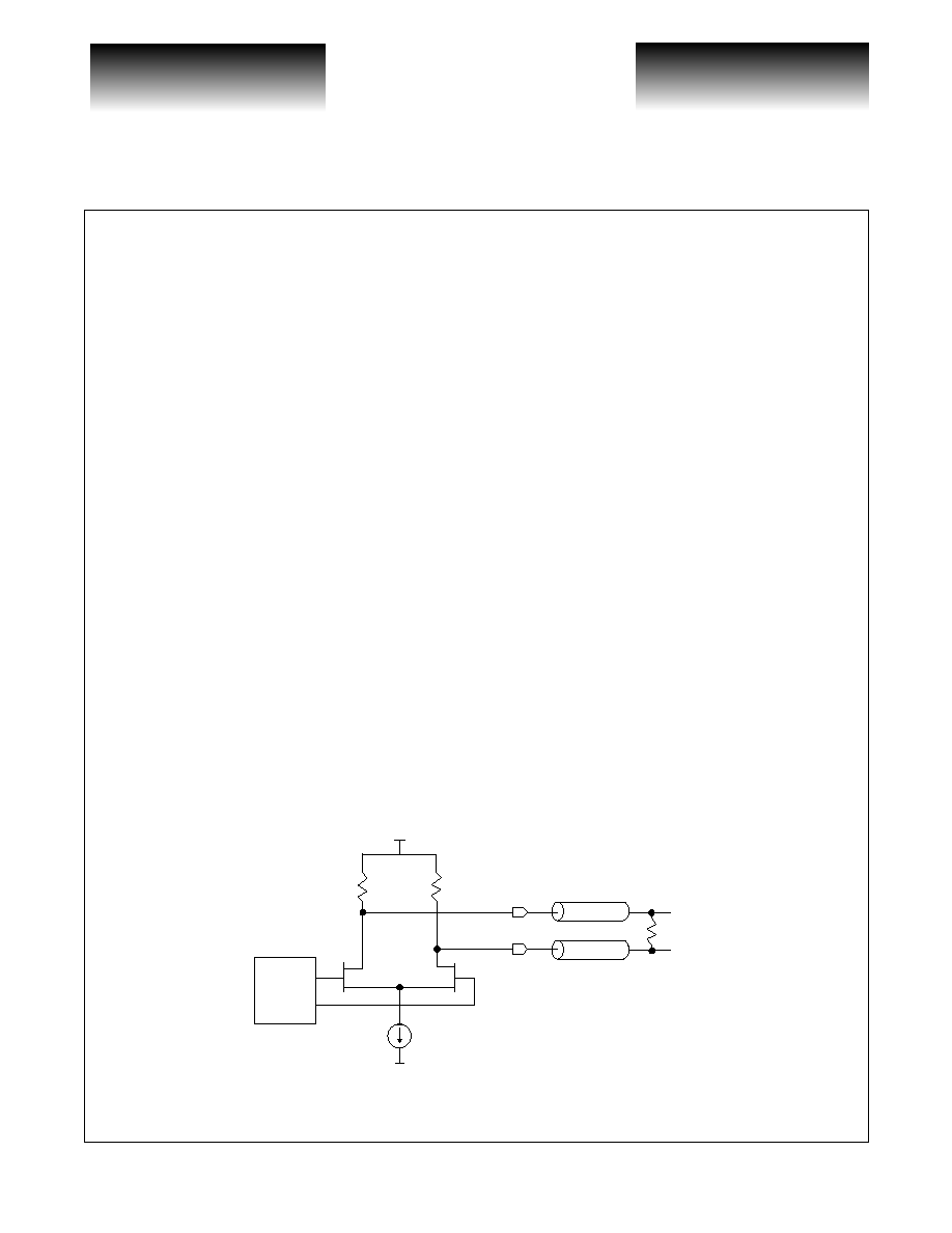
High-Speed Clock and High-Speed Data Inputs
The incoming high-speed data and high-speed clock are received by high-speed inputs RXIN and
RXCLKIN. The inputs are internally biased to accommodate AC-coupling.
The data input receiver is internally terminated by a center-tapped resistor network. For differential input
DC-coupling, the network is terminated to the appropriate termination voltage V
TERM
providing a 50
to
V
TERM
termination for both true and complement inputs. For differential input AC-coupling, the network is terminated
to V
TERM
via a blocking capacitor.
In most situations, these inputs will have high transition density and little DC offset. However, in cases
where this does not hold, direct DC connection is possible. All serial data and clock inputs have the same circuit
topology, as shown in Figure 16. The reference voltage is created by a resistor divider as shown. If the input sig-
nal is driven differentially and DC-coupled to the part, the mid-point of the input signal swing should be cen-
tered about this reference voltage and not exceed the maximum allowable amplitude. For single-ended, DC-
coupling operations, it is recommended that the user provides an external reference voltage which has better
temperature and power supply noise rejection than the on-chip resistor divider. The external reference should
have a nominal value equivalent to the common-mode switch point of the DC-coupled signal, and can be con-
nected to either side of the differential gate.
V
CC
= 3.3V
V
EE
= 0V
C
IN
Chip Boundary
C
IN
TYP = 100nF
C
AC
TYP = 100nF
Z
O
V
TERM
C
AC
50
50
C
IN
Z
O
1.65V
3k
3k
3k
3k
1.65V
©
VITESSE
SEMICONDUCTOR CORPORATION
Page 13
9/6/00
741 Calle Plano, Camarillo, CA 93012 ∑ 805/388-3700 ∑ FAX: 805/987-5896
VITESSE
SEMICONDUCTOR CORPORATION
Data Sheet
VSC8140
2.48832Gb/s 16:1 SONET/SDH
Transceiver with Integrated Clock Generator
G52251-0, Rev. 4.0
Supplies
The VSC8140 is specified as a PECL device with a single positive 3.3V supply. Should the user desire to
use the device in an ECL environment with a negative 3.3V supply, then V
CC
will be ground and V
EE
will be -
3.3V. If used with V
EE
tied to -3.3V, the TTL control signals are still referenced to V
EE
.
Decoupling of the power supplies is a critical element in maintaining the proper operation of the part. It is
recommended that the V
CC
power supply be decoupled using a 0.1
µ
F and 0.01
µ
F capacitor placed in parallel
on each V
CC
power supply pin as close to the package as possible. If room permits, a 0.001
µ
F capacitor should
also be placed in parallel with the 0.1
µ
F and 0.01
µ
F capacitors mentioned above. Recommended capacitors are
low-inductance ceramic SMT X7R devices. For the 0.1
µ
F capacitor, a 0603 package should be used. The
0.01
µ
F and 0.001
µ
F capacitors can be either 0603 or 0403 packages.
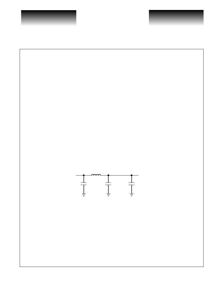
Extra care needs to be taken when decoupling the analog power supply pins (labeled V
CCANA
). In order to
maintain the optimal jitter and loop bandwidth characteristics of the PLL contained in the VSC8140, the analog
power supply pins should be filtered from the main power supply with a 10
µ
H C-L-C pi filter. If preferred, a
ferrite bead may be used to provide the isolation. The 0.1
µ
F and 0.01
µ
F decoupling capacitors are still required
and must be connected to the supply pins between the device and the C-L-C pi filter (or ferrite bead).
For low frequency decoupling, 47
µ
F tantalum low-inductance SMT caps are sprinkled over the board's
main +3.3V power supply and placed close to the C-L-C pi filter.
If the device is being used in an ECL environment with a -3.3V supply, then all references to decoupling
V
CC
must be changed to V
EE
, and all references to decoupling 3.3V must be changed to -3.3V.
Figure 17: PLL Power Supply Decoupling Scheme
Note: V
CC
can be tied to V
CCANA
V
EE
V
EEANA
V
CC
V
CCANA
V
CCANA
10
µ
H
0.1
µ
F
0.1
µ
F
0.01
µ
F

VITESSE
SEMICONDUCTOR CORPORATION
Data Sheet
VSC8140
2.48832Gb/s 16:1 SONET/SDH
Transceiver with Integrated Clock Generator
Page 14
©
VITESSE
SEMICONDUCTOR CORPORATION
741 Calle Plano, Camarillo, CA 93012 ∑ 805/388-3700 ∑ FAX: 805/987-5896
9/6/00
G52251-0, Rev. 4.0
AC Characteristics
Figure 18: Transmitter Parallel Data Timing Waveforms
Figure 19: Transmitter Serial Data and Clock Phase Timing
Figure 20: Transmitter Parity Timing
t
TXDSU
t
TXDH
Valid Data 1
TXCLK16I+
Parallel Data Clock Input
TXIN[0:15]+, TXPRTYIN
Parallel Data Inputs
TXCLK16O+
Parallel Data Clock Output
= don't care
Valid Data 2
D15
MSB
LSB
Time
D14
D13
TXOUT+
Differential Serial Data Output
TXCLKO+
Differential Clock Output
NOTE: Bit 15 (MSB) is transmitted first, Bit 0 (LSB) is transmitted last.
t
DH
t
PD
D1
D0
t
DV
t
D
t
D
TXCLK16I+
Parallel Data Clock Input
PARERR+
Data Valid Output

©
VITESSE
SEMICONDUCTOR CORPORATION
Page 15
9/6/00
741 Calle Plano, Camarillo, CA 93012 ∑ 805/388-3700 ∑ FAX: 805/987-5896
VITESSE
SEMICONDUCTOR CORPORATION
Data Sheet
VSC8140
2.48832Gb/s 16:1 SONET/SDH
Transceiver with Integrated Clock Generator
G52251-0, Rev. 4.0
Figure 21: Differential and Single-Ended Input / Output Voltage Measurement
Table 1: Transmitter AC Characteristics
Parameters
Description
Min
Typ
Max
Units
Conditions
T
D
TXCLK16I/TXCLK16O period
--
6.4
--
ns
--
T
TXDSU
Data setup time to the rising edge of
TXCLK16I+
0.75
--
--
ns
--
T
TXDH
Data hold time after the rising edge
of TXCLK16I+
1.0
--
--
ns
--
T
TXDOR
,
T
TXDOF
TXOUT± rise and fall time
--
--
120
ps
20% to 80% into 100
load.
See Figure 13.
TXCLK
D
Transmit clock duty cycle
40
--
60
%
--
t
TXCLK16R
,
t
TXCLK16F
TXCLK16O± rise and fall times
--
--
250
ps
See Figure 24
TXCLK16O
D
TXCLK16O± duty cycle
46
--
53
%
--
TXCLK16I
D
TXCLK16I± duty cycle
35
--
65
%
Assuming 10% distortion of
TXCLK16O.
RCK
D
Reference clock duty cycle
40
--
60
%
--
T
DV
Parallel data to DINVALID
--
3 t
D
+ 0.3
--
ns
--
t
DH
TXCLKO period
--
401.9
--
ps
--
t
PD
Center of output data eye from
falling edge of TXCLKO
-75
--
+75
ps
See Figure 19
Clock Multiplier Performance
T
DJ
Output data jitter
--
--
4
ps
RMS, tested to SONET
specification (12kHz to
20MHz) with 2ps RMS jitter
on REFCLK.
T
CJ
Output clock jitter
--
--
4
ps
RMS, tested to SONET
specification (12kHz to
20MHz) with 2ps RMS jitter
on REFCLK.
Jitter
tol
Jitter tolerance
--
--
--
--
Exceeds SONET/SDH mask
Tuning Range
-100
+100
ppm
Single
Ended
Swing
Differential
Swing
=
=
a
a
b
b
Differential swing is specified as equal in magnitude to single-ended swing.
* Differential swing
(
) is specified as | b - a | ( or | a - b | ), as is the single-ended swing.

VITESSE
SEMICONDUCTOR CORPORATION
Data Sheet
VSC8140
2.48832Gb/s 16:1 SONET/SDH
Transceiver with Integrated Clock Generator
Page 16
©
VITESSE
SEMICONDUCTOR CORPORATION
741 Calle Plano, Camarillo, CA 93012 ∑ 805/388-3700 ∑ FAX: 805/987-5896
9/6/00
G52251-0, Rev. 4.0
Figure 22: Receiver AC Timing Waveforms
Figure 23: Receiver Setup and Hold Time Requirements
Table 2: Receiver AC Characteristics
Parameters
Description
Min
Typ
Max
Units
Conditions
t
RXPDD
Data valid from falling edge of
RXCLK16O+
0
800
ps
--
t
RXPD32
RXCLK32O transition from
falling edge of RXCLK16O+
0
1.0
ns
--
t
RXDR
, t
RXDF
RXOUT[15:0]+/- rise and fall
times
--
300
ps
20% to 80% into DC termination.
See Figure 24.
t
RXCLKR
,
t
RXCLKF
RXCLK16O+/- rise and fall
times
--
250
ps
20% to 80% into 100
load.
See Figure 24.
RXCLK16O
D
RXCLK16O+/- duty cycle
distortion
45
55
% of
clock cycle
High-speed clock input at
2.48832GHz.
t
RXDSU
RXIN+ setup time with respect
to falling edge of RXCLKIN+
100
--
ps
--
t
RXDH
RXIN+ hold time with
respect to falling edge of
RXCLKIN+
75
--
ps
--
RXCLKIN
D
RXCLKIN+/- duty cycle
distortion
40
60
% of
clock cycle
--
t
RXDSU
t
RXPDD
t
RXPD32
Valid Data 1
RXCLK16O+
Parallel Data Clock Output
RXOUT[0:15]+
Parallel Data Outputs
RXCLK32O+
Parallel Data Clock Output
= don't care
Valid Data 2
D15
MSB
LSB
Time
D14
D13
RXIN+
Differential Serial Data Input
RXCLKIN+
Differential Clock Input
NOTE: Bit 15 (MSB) is received first, Bit 0 (LSB) is received last.
t
RXDSU
t
RXDH
D1
D0

©
VITESSE
SEMICONDUCTOR CORPORATION
Page 17
9/6/00
741 Calle Plano, Camarillo, CA 93012 ∑ 805/388-3700 ∑ FAX: 805/987-5896
VITESSE
SEMICONDUCTOR CORPORATION
Data Sheet
VSC8140
2.48832Gb/s 16:1 SONET/SDH
Transceiver with Integrated Clock Generator
G52251-0, Rev. 4.0
DC Characteristics
Table 3: DC Characteristics
(Over recommended operating conditions)
Parameters
Description
Min
Typ
Max
Units
Conditions
V
OHHSO
Output HIGH voltage (TXOUT,
TXCLKOUT)
V
CC
-0.40
--
V
CC
V
50
termination to V
CC
V
OLHSO
Output LOW voltage (TXOUT,
TXCLKOUT)
V
CC
-1.20
--
V
CC
-0.50
V
50
termination to V
CC
V
ODHSO
Output differential voltage
(TXCLKOUT)
450
600
1000
mV
100
termination between ±
output at load. See Figure 13.
Output differential voltage
(TXOUT)
500
600
1000
V
CMHSO
Output common-mode voltage
V
CC
-1.20
--
V
CC
-0.300
V
100
termination between ±
output at load. See Figure 13.
R
HSO
Back termination impedance
40
--
60
Guaranteed, but not tested
V
IHS
Serial input differential voltage
(RXIN, RXCLKIN)
200
--
--
mV
AC-coupled, internally
biased to (V
CC
+V
EE
)/2.
V
OHL
Output HIGH voltage (LVPECL)
V
CC
-1.020
--
V
CC
-0.700
V
See Figure 24
V
OL
Output LOW voltage (LVPECL)
V
CC
-2.000
--
V
CC
-1.620
V
See Figure 24
V
O
Low-speed output voltage single-
ended, peak-to-peak swing
(LVPECL)
600
--
1300
mV
See Figure 24
V
IH
Input HIGH voltage (LVPECL)
V
CC
-1.100
--
V
CC
-0.700
V
--
V
IL
Input LOW voltage(LVPECL)
V
CC
-2.0
--
V
CC
-1.540
V
--
I
IH
Input HIGH current (LVPECL)
--
--
200
µA
V
IN
=V
IH
(max)
I
IL
Input LOW current (LVPECL)
-50
--
--
µA
V
IN
=V
IL
(min)
R
i
Input Resistance (LVPECL)
10k
--
--
--
V
I
Input differential voltage
(LVPECL)
200
--
--
mV
--
V
CM
Input common-mode voltage
(LVPECL)
V
CC
-1.5
--
V
CC
-0.5
V
--
V
OH
Output HIGH voltage (TTL)
2.4
--
--
V
I
OH
= -1.0mA
V
OL
Output LOW voltage (TTL)
--
--
0.5
V
I
OL
= +1.0mA
V
IH
Input HIGH voltage (TTL)
2.0
--
5.5
V
--
V
IL
Input LOW voltage (TTL)
0.0
--
0.8
V
--
I
IH
Input HIGH Current (TTL)
--
--
500
µA
V
IN
= 2.4V
I
IL
Input LOW current (TTL)
--
--
-500
µA
V
IN
= 0.5V
V
CC
Supply voltage
3.14
--
3.47
V
3.3V± 5%
P
D
Power dissipation
--
2.25
2.75
W
Outputs open
I
CC
Supply current
--
--
800
mA
Outputs open

VITESSE
SEMICONDUCTOR CORPORATION
Data Sheet
VSC8140
2.48832Gb/s 16:1 SONET/SDH
Transceiver with Integrated Clock Generator
Page 18
©
VITESSE
SEMICONDUCTOR CORPORATION
741 Calle Plano, Camarillo, CA 93012 ∑ 805/388-3700 ∑ FAX: 805/987-5896
9/6/00
G52251-0, Rev. 4.0
Figure 24: Parametric Measurement Information
Absolute Maximum Ratings
(1)
Power Supply Voltage (V
CC
)...........................................................................................................-0.5V to +3.8V
DC Input Voltage (differential inputs).....................................................................................-0.5V to V
CC
+0.5V
DC Input Voltage (TTL inputs) .......................................................................................................-0.5V to +5.5V
DC Output Voltage (TTL outputs) .........................................................................................-0.5V to V
CC
+ 0.5V
Output Current (TTL outputs) .................................................................................................................. +/-50mA
Output Current (differential outputs).........................................................................................................+/-50mA
Case Temperature Under Bias ...................................................................................................... -55
o
C to +125
o
C
Recommended Operating Conditions
Power Supply Voltage (V
CC
)..................................................................................................................+3.3V+5%
Operating Temperature Range ...........................................................0
o
C Ambient to +110
o
C Case Temperature
NOTE: (1) CAUTION: Stresses listed under "Absolute Maximum Ratings" may be applied to devices one at a time without caus-
ing permanent damage. Functionality at or above the values listed is not implied. Exposure to these values for extended
periods may affect device reliability.
ESD Ratings
Proper ESD procedures should be used when handling this product. The VSC8140 is rated to the following
ESD voltages based on the human body model:
1. All pins are rated at or above 1500V.
PECL Rise and Fall Time
Serial Output Load
T
r
T
f
80%
20%
Z
0
= 50
50
V
CC
-2V
Parametric Test Load Circuit

©
VITESSE
SEMICONDUCTOR CORPORATION
Page 19
9/6/00
741 Calle Plano, Camarillo, CA 93012 ∑ 805/388-3700 ∑ FAX: 805/987-5896
VITESSE
SEMICONDUCTOR CORPORATION
Data Sheet
VSC8140
2.48832Gb/s 16:1 SONET/SDH
Transceiver with Integrated Clock Generator
G52251-0, Rev. 4.0
Package Pin Descriptions
Table 4: Package Pin Identification - 128 PQFP
Pin #
Name
I/O
Level
Description
1
OVERFLOW
O
TTL
FIFO overflow indication
2
VEET
--
GND typ.
TTL V
EE
power supply
3
VCCT
--
+3.3V typ.
TTL V
CC
power supply
4
VEE
--
GND typ.
Negative power supply
5
HSDREF
I
0V->3.3V
High-speed data input termination voltage reference
6
VEE
--
GND typ.
Negative power supply
7
RXIN+
I
HS
High-speed data input, true
8
RXIN-
I
HS
High-speed data input, complement
9
VCC
--
3.3V typ.
Positive power supply
10
VEE
--
GND typ.
Negative power supply
11
VEE
--
GND typ.
Negative power supply
12
VCC
--
3.3V typ.
Positive power supply
13
RXCLKIN-
I
HS
High-speed clock input, complement
14
HSCLKREF
I
0V->3.3V
High-speed clock input termination voltage reference
15
RXCLKIN+
I
HS
High-speed clock Input, true
16
VCC
--
3.3V typ.
Positive power supply
17
NC
--
--
No connect, leave unconnected
(1)
18
VCC
--
3.3V typ.
Positive power supply
19
VCC
--
3.3V typ.
Positive power supply
20
TXOUT+
O
HS
High-speed data output, true
21
TXOUT-
O
HS
High-speed data output, complement
22
VCC
--
3.3V typ.
Positive power supply
23
VEE
--
GND typ.
Negative power supply
24
VEE
--
GND typ.
Negative power supply
25
VEE
--
GND typ.
Negative power supply
26
VCC
--
3.3V typ.
Positive power supply
27
VCC
--
3.3V typ.
Positive power supply
28
TXCLKOUT+
O
HS
High-speed clock output, true
29
TXCLKOUT-
O
HS
High-speed clock output, complement
30
VCC
--
3.3V typ.
Positive power supply
31
VEEP_CLK
--
GND typ.
HS clock V
EE
power supply (tie to V
CC
for power down)
32
VEEP_CLK
--
GND typ.
HS clock V
EE
power supply (tie to V
CC
for power down)
33
VEE_PWRDN
I
GND typ.
HS clock V
EE
power supply (tie to V
CC
for power down)
34
VCC
--
3.3V typ.
Positive power supply
35
VCC
--
3.3V typ.
Positive power supply
36
VCC
--
3.3V typ.
Positive power supply

VITESSE
SEMICONDUCTOR CORPORATION
Data Sheet
VSC8140
2.48832Gb/s 16:1 SONET/SDH
Transceiver with Integrated Clock Generator
Page 20
©
VITESSE
SEMICONDUCTOR CORPORATION
741 Calle Plano, Camarillo, CA 93012 ∑ 805/388-3700 ∑ FAX: 805/987-5896
9/6/00
G52251-0, Rev. 4.0
37
VEE
--
GND typ.
Negative power supply
38
FACLOOP
I
TTL
Facility loopback, active high
39
LOOPTIM0
I
TTL
Enable internal looptiming operation, active high
40
PARMODE
I
TTL
Parity mode select
41
FIFORESET
I
TTL
Reset to align FIFO write and read pointers
42
LOOPTIM1
I
TTL
Enable external loop timing operation, active high
43
REF_FREQSEL
I
TTL
Reference clock input select
44
LPTIMCLK+
I
LVPECL
External loop timing clock, true
45
LPTIMCLK-
I
LVPECL
External loop timing clock, complement
46
VCC_ANA
--
+3.3V typ.
Positive power supplys for analog parts of CMU
47
VEE_ANA
--
GND typ.
Negative power supplys for analog parts of CMU
48
REFCLK+
I
LVPECL
Reference clock input, true
49
REFCLK-
I
LVPECL
Reference clock input, complement
50
VEE
--
GND typ.
Negative power supply
51
FILTAO
--
--
Loop filter pin - connect via capacitor to FILTAI (pin 53)
52
FILTAON
--
--
Loop filter pin - connect via capacitor to FILTAIN (pin 54)
53
FILTAI
--
--
Loop filter pin - connect via capacitor to FILTAO (pin 51)
54
FILTAIN
--
--
Loop filter pin - connect via capacitor to FILTAON (pin 52)
55
VCC
--
3.3V typ.
Positive power supply
56
TXCLK16O+
O
LVPECL
Low-speed clock output, true. A divide-by-16 version of the PLL
clock.
57
TXCLK16O-
O
LVPECL
Low-speed clock output, complement. A divide-by-16 version of the
PLL clock.
58
VEE
--
GND typ.
Negative power supply
59
TXCLK16I-
I
LVPECL
Low-speed clock input for latching low-speed data, complement
60
TXCLK16I+
I
LVPECL
Low-speed clock input for latching low-speed data, true
61
VCC
--
3.3V typ.
Positive power supply
62
TXPARITYIN
I
LVPECL
Transmitter parity bit input
63
TXIN15
I
LVPECL
Low-speed single-ended data (MSB)
(2)
64
TXIN14
I
LVPECL
Low-speed single-ended data
65
VEE
--
GND typ.
Negative power supply
66
VCC
--
3.3V typ.
Positive power supply
67
TXIN13
I
LVPECL
Low-speed single-ended data
68
TXIN12
I
LVPECL
Low-speed single-ended data
69
TXIN11
I
LVPECL
Low-speed single-ended data
70
TXIN10
I
LVPECL
Low-speed single-ended data
71
TXIN9
I
LVPECL
Low-speed single-ended data
Table 4: Package Pin Identification - 128 PQFP
Pin #
Name
I/O
Level
Description

©
VITESSE
SEMICONDUCTOR CORPORATION
Page 21
9/6/00
741 Calle Plano, Camarillo, CA 93012 ∑ 805/388-3700 ∑ FAX: 805/987-5896
VITESSE
SEMICONDUCTOR CORPORATION
Data Sheet
VSC8140
2.48832Gb/s 16:1 SONET/SDH
Transceiver with Integrated Clock Generator
G52251-0, Rev. 4.0
72
VEE
--
GND typ.
Negative power supply
73
TXIN8
I
LVPECL
Low-speed single-ended data
74
TXIN7
I
LVPECL
Low-speed single-ended data
75
TXIN6
I
LVPECL
Low-speed single-ended data
76
TXIN5
I
LVPECL
Low-speed single-ended data
77
TXIN4
I
LVPECL
Low-speed single-ended data
78
VCC
--
3.3V typ.
Positive power supply
79
TXIN3
I
LVPECL
Low-speed single-ended data
80
TXIN2
I
LVPECL
Low-speed single-ended data
81
VEE
--
GND typ.
Negative power supply
82
TXIN1
I
LVPECL
Low-speed single-ended data
83
TXIN0
I
LVPECL
Low-speed single-ended data (LSB)
(2)
84
VCC
--
3.3V typ.
Positive power supply
85
VREFIN
I
Voltage
Voltage reference for single-ended TXIN V
CM
or VREFOUT
86
VREFOUT
O
Voltage
Voltage reference for single-ended RXOUT (V
OH
+V
OL
)/2.
87
VCC
--
3.3V typ.
Positive power supply
88
RXOUT0
O
LVPECL
Low-speed single-ended data (LSB)
(2)
89
RXOUT1
O
LVPECL
Low-speed single-ended data
90
VEE
--
GND typ.
Negative power supply
91
RXOUT2
O
LVPECL
Low-speed single-ended data
92
RXOUT3
O
LVPECL
Low-speed single-ended data
93
VCC
--
3.3V typ.
Positive power supply
94
RXOUT4
O
LVPECL
Low-speed single-ended data
95
RXOUT5
O
LVPECL
Low-speed single-ended data
96
VCC
--
3.3V typ.
Positive power supply
97
RXOUT6
O
LVPECL
Low-speed single-ended data
98
RXOUT7
O
LVPECL
Low-speed single-ended data
99
VEE
--
GND typ.
Negative power supply
100
RXOUT8
O
LVPECL
Low-speed single-ended data
101
RXOUT9
O
LVPECL
Low-speed single-ended data
102
VCC
--
3.3V typ.
Positive power supply
103
VCC
--
3.3V typ.
Positive power supply
104
RXOUT10
O
LVPECL
Low-speed single-ended data
105
RXOUT11
O
LVPECL
Low-speed single-ended data
106
RXOUT12
O
LVPECL
Low-speed single-ended data
107
VCC
--
3.3V typ.
Positive power supply
108
RXOUT13
O
LVPECL
Low-speed single-ended data
Table 4: Package Pin Identification - 128 PQFP
Pin #
Name
I/O
Level
Description

VITESSE
SEMICONDUCTOR CORPORATION
Data Sheet
VSC8140
2.48832Gb/s 16:1 SONET/SDH
Transceiver with Integrated Clock Generator
Page 22
©
VITESSE
SEMICONDUCTOR CORPORATION
741 Calle Plano, Camarillo, CA 93012 ∑ 805/388-3700 ∑ FAX: 805/987-5896
9/6/00
G52251-0, Rev. 4.0
NOTES: (1) No connect (NC) pin must be left unconnected. Connecting this pin to either the positive or negative power supply
rails may cause improper operation or failure of the device; or in extreme cases, cause permanent damage to the device.
(2) There has been a change in the naming of the pins of the Low-Speed Parallel Receive and Transmit pins of the
VSC8140. RXOUT0; pin 88 (MSB) has been changed to RXOUT15; pin 111 (MSB) and TXIN15; pin 63 (LSB) has been
changed to TXIN0; pin 83 (LSB).
109
RXOUT14
O
LVPECL
Low-speed single-ended data
110
VEE
--
GND typ.
Negative power supply
111
RXOUT15
O
LVPECL
Low-speed single-ended data (MSB)
(2)
112
RXPARITYOUT
O
LVPECL
Receiver parity bit output
113
VCC
--
3.3V typ.
Positive power supply
114
RXCLK16O-
O
LVPECL
Parallel clock output (155.52MHz), complement
115
RXCLK16O+
O
LVPECL
Parallel clock output (155.52MHz), true
116
VEE
--
GND typ.
Negative power supply
117
VCC
--
3.3V typ.
Positive power supply
118
RXCLK16_32O-
O
LVPECL
Divide-by-16 or -32 clock output, complement
119
RXCLK16_32O+
O
LVPECL
Divide-by-16 or -32 clock output, true
120
CLK128O-
O
LVPECL
Divide-by-128 clock output, complement
121
CLK128O+
O
LVPECL
Divide-by-128 clock output, true
122
VCC
--
3.3V typ.
Positive power supply
123
RXCLKO_FREQSEL
I
TTL
RXCLKO16_32 frequency select
124
LOS
I
TTL
Loss of Signal control
125
POL
I
TTL
Polarity Signal Control
126
EQULOOP
I
TTL
Equipment loopback, active high
127
VCC
--
3.3V typ.
Positive power supply
128
PARERR
O
TTL
Parity error output
Table 4: Package Pin Identification - 128 PQFP
Pin #
Name
I/O
Level
Description

©
VITESSE
SEMICONDUCTOR CORPORATION
Page 23
9/6/00
741 Calle Plano, Camarillo, CA 93012 ∑ 805/388-3700 ∑ FAX: 805/987-5896
VITESSE
SEMICONDUCTOR CORPORATION
Data Sheet
VSC8140
2.48832Gb/s 16:1 SONET/SDH
Transceiver with Integrated Clock Generator
G52251-0, Rev. 4.0
Package Information
STANDOFF
LEAD COPLANARITY
MAX.
0.17
.25
A
L
A1
A1
A2
R1
R
1
b
e
A
10
∞
TYP.
10
∞
TYP.
TOP VIEW
EXPOSED
HEATSINK
EXPOSED
INTRUSION
0.127 MAX.
RAD. 2.92
±
.50
(2)
2.54
±
.50
PIN 128
PIN 1
E1
E
D1
D
Notes: 1)
Drawing is not to scale
2)
All dimensions in mm
3)
Package represented is
also used for the 64,
80, & 100 PQFP packages.
Pin count drawn does
not reflect the 128 Package.
PIN 38
PIN 64
PIN 102
NOTES:
128 PQFP Package Drawings
Package #: 101-322-5
Issue #: 2
Key
mm
Tolerance
A
2.35
MAX
A1
0.25
MAX
A2
2.00
+.10
D
17.20
±.20
D1
14.00
±.10
E
23.20
±.20
E1
20.00
±.10
L
.88
+.15/-.10
e
.50
BASIC
b
.22
±.05
q
0∞-7∞
R
.30
TYP
R1
.20
TYP

VITESSE
SEMICONDUCTOR CORPORATION
Data Sheet
VSC8140
2.48832Gb/s 16:1 SONET/SDH
Transceiver with Integrated Clock Generator
Page 24
©
VITESSE
SEMICONDUCTOR CORPORATION
741 Calle Plano, Camarillo, CA 93012 ∑ 805/388-3700 ∑ FAX: 805/987-5896
9/6/00
G52251-0, Rev. 4.0
Package Pin Descriptions
Table 5: Package Pin Identification - 208 BGA
Pin #
Name
I/O
Level
Description
B17
OVERFLOW
O
TTL
FIFO overflow indication
B16
VEET
--
GND typ.
TTL V
EE
power supply
B15
VCCT
--
+3.3V typ.
TTL V
CC
power supply
C14
VEE
--
GND typ.
Negative power supply
D13
HSDREF
I
0V->3.3V
High-speed data input termination voltage reference
A16
VEE
--
GND typ.
Negative power supply
B14
RXIN+
I
HS
High-speed data input, true
B13
RXIN-
I
HS
High-speed data input, complement
A14
VCC
--
3.3V typ.
Positive power supply
A13
VEE
--
GND typ.
Negative power supply
D11
VEE
--
GND typ.
Negative power supply
C11
VCC
--
3.3V typ.
Positive power supply
B11
RXCLKIN-
I
HS
High-speed clock input, complement
D10
HSCLKREF
I
0V->3.3V
High-speed clock input termination voltage reference
B10
RXCLKIN+
I
HS
High-speed clock input, true
A10
VCC
--
3.3V typ.
Positive power supply
B9
VCC
--
3.3V typ.
Positive power supply
D9
VCC
--
3.3V typ.
Positive power supply
A9
TXOUT+
O
HS
High-speed data output, true
A8
TXOUT-
O
HS
High-speed data output, complement
C8
VCC
--
3.3V typ.
Positive power supply
D8
VEE
--
GND typ.
Negative power supply
A7
VEE
--
GND typ.
Negative power supply
A6
VEE
--
GND typ.
Negative power supply
D7
VCC
--
3.3V typ.
Positive power supply
A5
VCC
--
3.3V typ.
Positive power supply
A4
TXCLKOUT+
O
HS
High-speed clock output, true
A3
TXCLKOUT-
O
HS
High-speed clock output, complement
B4
VCC
--
3.3V typ.
Positive power supply
D5
VEEP_CLK
--
GND typ.
HS clock V
EE
power supply (tie to V
CC
for power down)
A2
VEEP_CLK
--
GND typ.
HS clock V
EE
power supply (tie to V
CC
for power down)
A1
VEE_PWRDN
I
GND typ.
HS clock V
EE
power supply (tie to V
CC
for power down)
C4
VCC
--
3.3V typ.
Positive power supply

©
VITESSE
SEMICONDUCTOR CORPORATION
Page 25
9/6/00
741 Calle Plano, Camarillo, CA 93012 ∑ 805/388-3700 ∑ FAX: 805/987-5896
VITESSE
SEMICONDUCTOR CORPORATION
Data Sheet
VSC8140
2.48832Gb/s 16:1 SONET/SDH
Transceiver with Integrated Clock Generator
G52251-0, Rev. 4.0
B3
VCC
--
3.3V typ.
Positive power supply
D4
VCC
--
3.3V typ.
Positive power supply
C3
VEE
--
GND typ.
Negative power supply
C1
FACLOOP
I
TTL
Facility loopback, active high
F4
LOOPTIM0
I
TTL
Enable internal looptiming operation, active high
F3
PARMODE
I
TTL
Parity mode select
D1
FIFORESET
I
TTL
Reset to align FIFO write and read pointers
E1
LOOPTIM1
I
TTL
Enable external loop timing operation, active high
G4
REF_FREQSEL
I
TTL
Reference clock input select
G3
VEE
--
GND typ.
Negative power supply
F2
LPTIMCLK+
I
LVPECL
External loop timing clock, true
G2
LPTIMCLK-
I
LVPECL
External loop timing clock, complement
F1
VCC_ANA
--
+3.3V typ.
Positive power supplies for analog parts of CMU
H3
VEE_ANA
--
GND typ.
Negative power supplies for analog parts of CMU
H2
REFCLK+
I
LVPECL
Reference clock input, true
G1
REFCLK-
I
LVPECL
Reference clock input,complement
H1
VEE
--
GND typ.
Negative power supply
J2
VCC
--
3.3V typ.
Positive power supply
J4
FILTAO
--
--
Loop filter pin - connect via capacitor to FILTAI (pin 53)
J3
FILTAON
--
--
Loop filter pin - connect via capacitor to FILTAIN (pin 54)
K1
FILTAI
--
--
Loop filter pin - connect via capacitor to FILTAO (pin 51)
K2
FILTAIN
--
--
Loop filter pin - connect via capacitor to FILTAON (pin 52)
K3
VCC
--
3.3V typ.
Positive power supply
K4
TXCLK16O+
O
LVPECL
Low-speed clock output, true. A divide-by-16 version of the PLL
clock.
L1
TXCLK16O-
O
LVPECL
Low-speed clock output, complement. A divide-by-16 version of the
PLL clock.
M1
VEE
--
GND typ.
Negative power supply
L2
TXCLK16I-
I
LVPECL
Low-speed clock input for latching low-speed data, complement
L3
TXCLK16I+
I
LVPECL
Low-speed clock input for latching low-speed data, true
L4
VCC
--
3.3V typ.
Positive power supply
M2
TXPARITYIN
I
LVPECL
Transmitter parity bit input
M3
TXIN15
I
LVPECL
Low-speed single-ended data (MSB)
(1)
M4
TXIN14
I
LVPECL
Low-speed single-ended data
P1
VEE
--
GND typ.
Negative power supply
Table 5: Package Pin Identification - 208 BGA
Pin #
Name
I/O
Level
Description

VITESSE
SEMICONDUCTOR CORPORATION
Data Sheet
VSC8140
2.48832Gb/s 16:1 SONET/SDH
Transceiver with Integrated Clock Generator
Page 26
©
VITESSE
SEMICONDUCTOR CORPORATION
741 Calle Plano, Camarillo, CA 93012 ∑ 805/388-3700 ∑ FAX: 805/987-5896
9/6/00
G52251-0, Rev. 4.0
T3
VCC
--
3.3V typ.
Positive power supply
P5
TXIN13
I
LVPECL
Low-speed single-ended data
R5
TXIN12
I
LVPECL
Low-speed single-ended data
T4
TXIN11
I
LVPECL
Low-speed single-ended data
P6
TXIN10
I
LVPECL
Low-speed single-ended data
T5
TXIN9
I
LVPECL
Low-speed single-ended data
R6
VEE
--
GND typ.
Negative power supply
U5
TXIN8
I
LVPECL
Low-speed single-ended data
R7
TXIN7
I
LVPECL
Low-speed single-ended data
T6
TXIN6
I
LVPECL
Low-speed single-ended data
U6
TXIN5
I
LVPECL
Low-speed single-ended data
P8
TXIN4
I
LVPECL
Low-speed single-ended data
R8
VCC
--
3.3V typ.
Positive power supply
T8
TXIN3
I
LVPECL
Low-speed single-ended data
U7
TXIN2
I
LVPECL
Low-speed single-ended data
U8
VEE
--
GND typ.
Negative power supply
T9
TXIN1
I
LVPECL
Low-speed single-ended data
P9
TXIN0
I
LVPECL
Low-speed single-ended data (LSB)
(1)
R9
VCC
--
3.3V typ.
Positive power supply
U9
VREFIN
I
Voltage
Voltage reference for single-ended TXIN V
CM
or VREFOUT
U10
VREFOUT
O
Voltage
Voltage reference for single-ended RXOUT (V
OH
+V
OL
)/2
T10
VCC
--
3.3V typ.
Positive power supply
R10
RXOUT0
O
LVPECL
Low-speed single-ended data (LSB)
(1)
P10
RXOUT1
O
LVPECL
Low-speed single-ended data
U11
VEE
--
GND typ.
Negative power supply
U12
RXOUT2
O
LVPECL
Low-speed single-ended data
T11
RXOUT3
O
LVPECL
Low-speed single-ended data
R11
VCC
--
3.3V typ.
Positive power supply
P11
RXOUT4
O
LVPECL
Low-speed single-ended data
U13
RXOUT5
O
LVPECL
Low-speed single-ended data
T12
VCC
--
3.3V typ.
Positive power supply
T13
RXOUT6
O
LVPECL
Low-speed single-ended data
R12
RXOUT7
O
LVPECL
Low-speed single-ended data
P12
VEE
--
GND typ.
Negative power supply
Table 5: Package Pin Identification - 208 BGA
Pin #
Name
I/O
Level
Description

©
VITESSE
SEMICONDUCTOR CORPORATION
Page 27
9/6/00
741 Calle Plano, Camarillo, CA 93012 ∑ 805/388-3700 ∑ FAX: 805/987-5896
VITESSE
SEMICONDUCTOR CORPORATION
Data Sheet
VSC8140
2.48832Gb/s 16:1 SONET/SDH
Transceiver with Integrated Clock Generator
G52251-0, Rev. 4.0
U14
RXOUT8
O
LVPECL
Low-speed single-ended data
U15
RXOUT9
O
LVPECL
Low-speed single-ended data
R13
VCC
--
3.3V typ.
Positive power supply
N16
VCC
--
3.3V typ.
Positive power supply
P17
RXOUT10
O
LVPECL
Low-speed single-ended data
L14
RXOUT11
O
LVPECL
Low-speed single-ended data
L15
RXOUT12
O
LVPECL
Low-speed single-ended data
M16
VCC
--
3.3V typ.
Positive power supply
L16
RXOUT13
O
LVPECL
Low-speed single-ended data
M17
RXOUT14
O
LVPECL
Low-speed single-ended data
K14
VEE
--
GND typ.
Negative power supply
K15
RXOUT15
O
LVPECL
Low-speed single-ended data (MSB)
(1)
K16
RXPARITYOUT
O
LVPECL
Receiver Parity bit output
L17
VCC
--
3.3V typ.
Positive power supply
J17
RXCLK16O-
O
LVPECL
Parallel clock output (155.52MHz), complement
H17
RXCLK16O+
O
LVPECL
Parallel clock output (155.52MHz), true
H16
VEE
--
GND typ.
Negative power supply
H15
VCC
--
3.3V typ.
Positive power supply
H14
RXCLK16_32O-
O
LVPECL
Divide-by-16 or -32 clock output, complement
G17
RXCLK16_32O+
O
LVPECL
Divide-by-16 or -32 clock output, true
F17
CLK128O-
O
LVPECL
Divide-by-128 clock output, complement
G16
CLK128O+
O
LVPECL
Divide-by-128 clock output, true
G15
VCC
--
3.3V typ.
Positive power supply
G14
RXCLKO_FREQSEL
I
TTL
RXCLKO16_32 frequency select
D17
LOS
I
TTL
Loss of Signal control
C17
POL
I
TTL
Polarity Signal Control
E15
EQULOOP
I
TTL
Equipment loopback, active high
D16
VCC
--
3.3V typ.
Positive power supply
E14
PARERR
O
TTL
Parity error output
A17
NC
--
--
No connect, leave unconnected
(2)
A15
NC
--
--
No connect, leave unconnected
(2)
A12
NC
--
--
No connect, leave unconnected
(2)
A11
NC
--
--
No connect, leave unconnected
(2)
B12
NC
--
--
No connect, leave unconnected
(2)
B8
NC
--
--
No connect, leave unconnected
(2)
Table 5: Package Pin Identification - 208 BGA
Pin #
Name
I/O
Level
Description

VITESSE
SEMICONDUCTOR CORPORATION
Data Sheet
VSC8140
2.48832Gb/s 16:1 SONET/SDH
Transceiver with Integrated Clock Generator
Page 28
©
VITESSE
SEMICONDUCTOR CORPORATION
741 Calle Plano, Camarillo, CA 93012 ∑ 805/388-3700 ∑ FAX: 805/987-5896
9/6/00
G52251-0, Rev. 4.0
B7
NC
--
--
No connect, leave unconnected
(2)
B6
NC
--
--
No connect, leave unconnected
(2)
B5
NC
--
--
No connect, leave unconnected
(2)
B2
NC
--
--
No connect, leave unconnected
(2)
B1
NC
--
--
No connect, leave unconnected
(2)
C16
NC
--
--
No connect, leave unconnected
(2)
C15
NC
--
--
No connect, leave unconnected
(2)
C13
NC
--
--
No connect, leave unconnected
(2)
C12
NC
--
--
No connect, leave unconnected
(2)
C10
NC
--
--
No connect, leave unconnected
(2)
C9
NC
--
--
No connect, leave unconnected
(2)
C7
NC
--
--
No connect, leave unconnected
(2)
C6
NC
--
--
No connect, leave unconnected
(2)
C5
NC
--
--
No connect, leave unconnected
(2)
C2
NC
--
--
No connect, leave unconnected
(2)
D15
NC
--
--
No connect, leave unconnected
(2)
D14
NC
--
--
No connect, leave unconnected
(2)
D12
NC
--
--
No connect, leave unconnected
(2)
D6
NC
--
--
No connect, leave unconnected
(2)
D3
NC
--
--
No connect, leave unconnected
(2)
D2
NC
--
--
No connect, leave unconnected
(2)
E17
NC
--
--
No connect, leave unconnected
(2)
E16
NC
--
--
No connect, leave unconnected
(2)
E4
NC
--
--
No connect, leave unconnected
(2)
E3
NC
--
--
No connect, leave unconnected
(2)
E2
NC
--
--
No connect, leave unconnected
(2)
F16
NC
--
--
No connect, leave unconnected
(2)
F15
NC
--
--
No connect, leave unconnected
(2)
F14
NC
--
--
No connect, leave unconnected
(2)
H4
NC
--
--
No connect, leave unconnected
(2)
J16
NC
--
--
No connect, leave unconnected
(2)
J15
NC
--
--
No connect, leave unconnected
(2)
J14
NC
--
--
No connect, leave unconnected
(2)
J1
NC
--
--
No connect, leave unconnected
(2)
K17
NC
--
--
No connect, leave unconnected
(2)
Table 5: Package Pin Identification - 208 BGA
Pin #
Name
I/O
Level
Description
©
VITESSE
SEMICONDUCTOR CORPORATION
Page 29
9/6/00
741 Calle Plano, Camarillo, CA 93012 ∑ 805/388-3700 ∑ FAX: 805/987-5896
VITESSE
SEMICONDUCTOR CORPORATION
Data Sheet
VSC8140
2.48832Gb/s 16:1 SONET/SDH
Transceiver with Integrated Clock Generator
G52251-0, Rev. 4.0
M15
NC
--
--
No connect, leave unconnected
(2)
M14
NC
--
--
No connect, leave unconnected
(2)
N17
NC
--
--
No connect, leave unconnected
(2)
N15
NC
--
--
No connect, leave unconnected
(2)
N14
NC
--
--
No connect, leave unconnected
(2)
N4
NC
--
--
No connect, leave unconnected
(2)
N3
NC
--
--
No connect, leave unconnected
(2)
N2
NC
--
--
No connect, leave unconnected
(2)
N1
NC
--
--
No connect, leave unconnected
(2)
P16
NC
--
--
No connect, leave unconnected
(2)
P15
NC
--
--
No connect, leave unconnected
(2)
P14
NC
--
--
No connect, leave unconnected
(2)
P13
NC
--
--
No connect, leave unconnected
(2)
P7
NC
--
--
No connect, leave unconnected
(2)
P4
NC
--
--
No connect, leave unconnected
(2)
P3
NC
--
--
No connect, leave unconnected
(2)
P2
NC
--
--
No connect, leave unconnected
(2)
R17
NC
--
--
No connect, leave unconnected
(2)
R16
NC
--
--
No connect, leave unconnected
(2)
R15
NC
--
--
No connect, leave unconnected
(2)
R14
NC
--
--
No connect, leave unconnected
(2)
R4
NC
--
--
No connect, leave unconnected
(2)
R3
NC
--
--
No connect, leave unconnected
(2)
R2
NC
--
--
No connect, leave unconnected
(2)
R1
NC
--
--
No connect, leave unconnected
(2)
T17
NC
--
--
No connect, leave unconnected
(2)
T16
NC
--
--
No connect, leave unconnected
(2)
T15
NC
--
--
No connect, leave unconnected
(2)
T14
NC
--
--
No connect, leave unconnected
(2)
T7
NC
--
--
No connect, leave unconnected
(2)
T2
NC
--
--
No connect, leave unconnected
(2)
T1
NC
--
--
No connect, leave unconnected
(2)
U17
NC
--
--
No connect, leave unconnected
(2)
U16
NC
--
--
No connect, leave unconnected
(2)
U4
NC
--
--
No connect, leave unconnected
(2)
Table 5: Package Pin Identification - 208 BGA
Pin #
Name
I/O
Level
Description

VITESSE
SEMICONDUCTOR CORPORATION
Data Sheet
VSC8140
2.48832Gb/s 16:1 SONET/SDH
Transceiver with Integrated Clock Generator
Page 30
©
VITESSE
SEMICONDUCTOR CORPORATION
741 Calle Plano, Camarillo, CA 93012 ∑ 805/388-3700 ∑ FAX: 805/987-5896
9/6/00
G52251-0, Rev. 4.0
NOTES: (1) There has been a change in the naming of the pins of the Low-Speed Parallel Receive and Transmit pins of the
VSC8140. RXOUT0; pin R10 (MSB) has been changed to RXOUT15; pin K15 (MSB) and TXIN15; pin M3 (LSB) has
been changed to TXIN0; pin P9 (LSB).
(2) No connect (NC) pins must be left unconnected. Connecting any of these pins to either the positive or negative power
supply rails may cause improper operation or failure of the device; or in extreme cases, cause permanent damage to the
device.
U3
NC
--
--
No connect, leave unconnected
(2)
U2
NC
--
--
No connect, leave unconnected
(2)
U1
NC
--
--
No connect, leave unconnected
(2)
Table 5: Package Pin Identification - 208 BGA
Pin #
Name
I/O
Level
Description
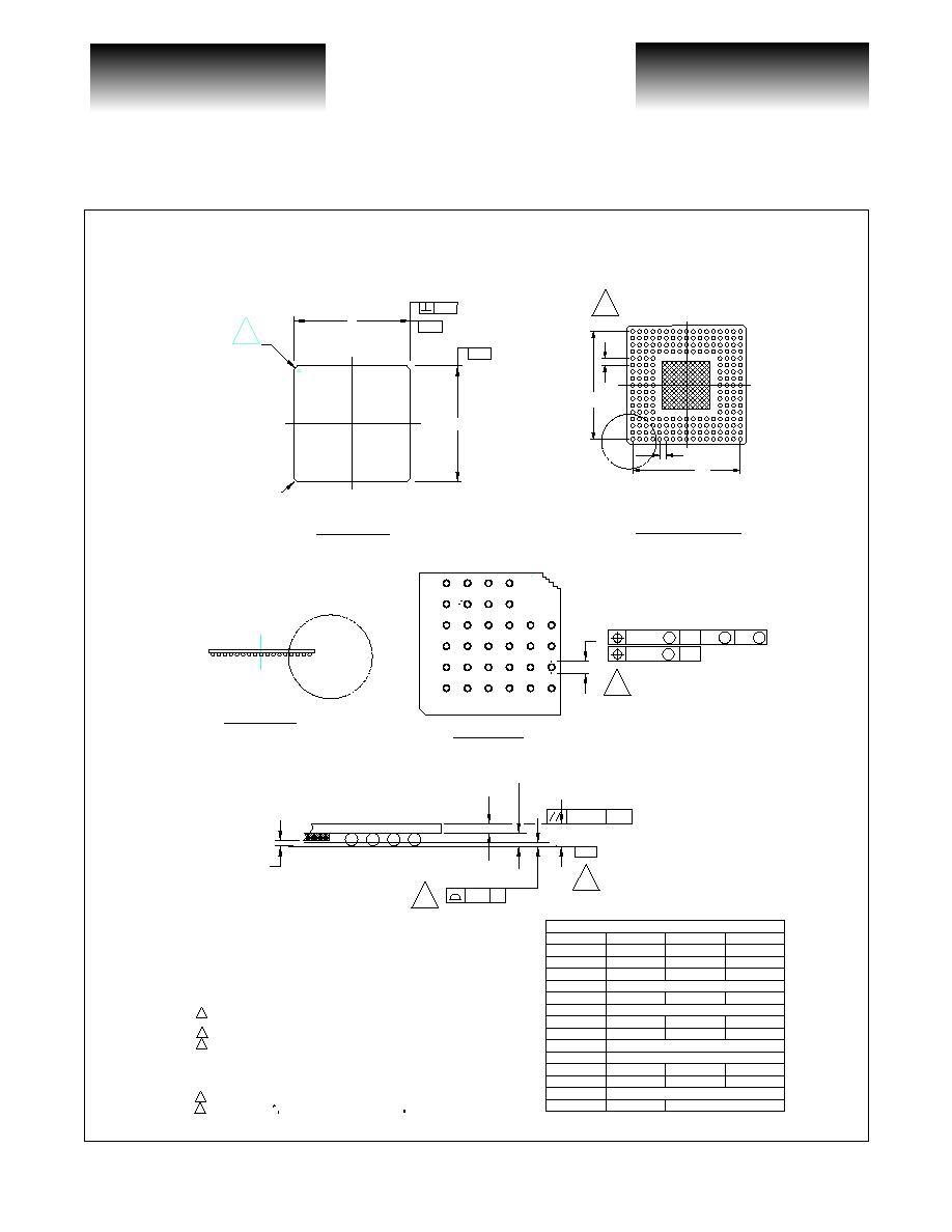
©
VITESSE
SEMICONDUCTOR CORPORATION
Page 31
9/6/00
741 Calle Plano, Camarillo, CA 93012 ∑ 805/388-3700 ∑ FAX: 805/987-5896
VITESSE
SEMICONDUCTOR CORPORATION
Data Sheet
VSC8140
2.48832Gb/s 16:1 SONET/SDH
Transceiver with Integrated Clock Generator
G52251-0, Rev. 4.0
Package Information
11. 45 DEG. 0.5 MM CHAMFER CORNER AND WHITE DOT FOR PIN1 IDENTIFICATION
10. BILATERIAL TOLERANCE ZONE IS APPLIED TO EACH SIDE OF PACKAGE BODY
8. CAVITY DEPTH VARIOUS WITH DIE THICKNESS
7. PACKAGE SURFACE SHALL BE BLACK OXIDE.
9. SUBSTRATE MATERIAL BASE IS COPPER.
BALLS AFTER DEPOPULATING.
5.
SPHERICAL CROWNS OF THE SOLDER BALLS.
6. PRIMARY DATUM -C- AND SEATING PLANE ARE DEFINED BY THE
DIMENSION "aaa" IS MEASURED PARALLEL TO PRIMARY DATUM -C- .
PARALLEL TO PRIMARY DATUM -C- .
4. "b" IS MEASURED AT THE MAXIMUM SOLDER BALL DIAMETER
AND SYMBOL "N" IS THE MAXIMUM ALLOWABLE NUMBER OF
3. "M" REPRESENTS THE BASIC SOLDER BALL MATRIX SIZE,
2. "e" REPRESENTS THE BASIC SOLDER BALL GRID PITCH.
1. ALL DIMENSIONS ARE IN MILLIMETERS.
NOTES:
10
e
c
c
c
c
e
D1
E1
45 DEGREE 0.5MM CHAMFER
0.10 S C
0.30 S C A S B S
A
CORNER
(4 PLCS)
E
D
11
P
b
DETAIL B
DETAIL A
SIDE VIEW
TOP VIEW
BOTTOM VIEW
DETAIL A
DETAIL B
6
5
4
-C-
aaa C
A1
c
U
T
R
P
N
M
L
K
J
H
G
F
E
D
C
B
A
17
16
15
14
13
12
11
10
9
8
7
6
5
4
3
2
1
-B-
0.10
-A-
0.15
20.32 (BSC.)
23.00
0.70
0.65
0.60
0.85
0.65
0.90
0.75
1.45
1.55
P
ccc
208
N
1.27 TYP.
0.95
0.85
17
20.32 (BSC.)
23.00
1.65
e
aaa
c
b
M
E1
E
D1
D
A1
A
MAX.
NOM.
MIN.
REF.
DIMENSIONAL REFERENCES
0.25
0.25
23.20
22.80
23.20
22.80
208 TBGA Package Drawings

VITESSE
SEMICONDUCTOR CORPORATION
Data Sheet
VSC8140
2.48832Gb/s 16:1 SONET/SDH
Transceiver with Integrated Clock Generator
Page 32
©
VITESSE
SEMICONDUCTOR CORPORATION
741 Calle Plano, Camarillo, CA 93012 ∑ 805/388-3700 ∑ FAX: 805/987-5896
9/6/00
G52251-0, Rev. 4.0
Package Thermal Considerations
This package has been enhanced with a copper heat slug to provide a low thermal resistance path from the
die to the exposed surface of the heat spreader. The thermal resistance is shown in the following table:
Table 6: Thermal Resistance
Thermal Resistance with Airflow
Shown in the table below is the thermal resistance with airflow. This thermal resistance value reflects all the
thermal paths including through the leads in an environment where the leads are exposed. The temperature dif-
ference between the ambient airflow temperature and the case temperature should be the worst case power of
the device multiplied by the thermal resistance.
Table 7: Thermal Resistance with Airflow
Maximum Ambient Temperature without Heatsink
The worst case ambient temperature without use of a heatsink is given by the equation:
where:
CA
Theta case to ambient at appropriate airflow
A(MAX)
Ambient Air temperature
C(MAX
)
Case temperature (110
o
C for VSC8140)
P
(MAX)
Power (2.75 W for VSC8140)
Symbol
Description
∞
C/W - (BGA)
∞
C/W (PQFP)
jc
Thermal resistance from junction to case.
2.2
1.34
ca
Thermal resistance from case to ambient with no airflow,
including conduction through the leads.
18.5
25.0
Airflow
ca
(
o
C/W
) (BGA)
ca
(
o
C/W
) (PQFP)
100 lfpm
18
21
200 lfpm
17
18
400 lfpm
16
16
T
A MAX
(
)
T
C MAX
(
)
P
≠
MAX
(
)
CA
=

©
VITESSE
SEMICONDUCTOR CORPORATION
Page 33
9/6/00
741 Calle Plano, Camarillo, CA 93012 ∑ 805/388-3700 ∑ FAX: 805/987-5896
VITESSE
SEMICONDUCTOR CORPORATION
Data Sheet
VSC8140
2.48832Gb/s 16:1 SONET/SDH
Transceiver with Integrated Clock Generator
G52251-0, Rev. 4.0
The results of this calculation are listed below:
Table 8: Maximum Ambient Air Temperature without Heatsink
Note that ambient air temperature varies throughout the system based on the positioning and magnitude of
heat sources and the direction of air flow.
Surface Mount Solderability
The make-up of each lead on the PQFP and TBGA package is 85% Tin and 15% Lead. The solderability
requirements for the various methods is described below.
Reflow Soldering
This is the suitable method of soldering for these components. When using reflow soldering to mount the
IC package, solder paste (a suspension of fine solder particles, flux, and binding agent) is required to be applied
to the printed-circuit board by screen printing, stenciling, or pressure-syringe dispensing before package place-
ment.
Throughput times (this includes preheating, soldering, and cooling) are shown in Table 9.
Table 9: Reflow Running Profile
Wave Soldering
Conventional single wave soldering is not recommended for surface mount devices or printed circuit boards
with high component density, as solder bridging and non-wetting can present problems. Double-wave soldering
can be used, only if the method comprises a turbulent wave with high upward pressure followed by a smooth
laminar wave and the footprint must incorporate solder thieves at the downstream end. The package must be
fixed with a droplet of adhesive during placement before soldering. After the adhesive is cured, the package can
be soldered.
Airflow
o
C (TBGA)
o
C (PQFP)
None
59
41
100 lfpm
60
52
200 lfpm
63
60
400 lfpm
66
66
Condition
TBGA
PQFP
Average ramp up (from 183
o
C to peak temperature)
1.553
o
C/sec
1.5432
o
C/sec
Average ramp down (from peak to 183
o
C)
-1.152
o
C/sec
-1.085
o
C/sec
Preheat Temperature (125
o
C)
77 sec
79 sec
Temperature maintained above 183
o
C
80 sec
80 sec
Time within 5
o
C of actual peak temperature
19 sec
19 sec
Peak Temperature Range
220-225
o
C
220-225
o
C
Peak Temperature
224
o
C
224
o
C
Time 25
o
C to Peak
Temperature
233 sec
228 sec

VITESSE
SEMICONDUCTOR CORPORATION
Data Sheet
VSC8140
2.48832Gb/s 16:1 SONET/SDH
Transceiver with Integrated Clock Generator
Page 34
©
VITESSE
SEMICONDUCTOR CORPORATION
741 Calle Plano, Camarillo, CA 93012 ∑ 805/388-3700 ∑ FAX: 805/987-5896
9/6/00
G52251-0, Rev. 4.0
Manual Soldering
When manually soldering the device to the printed circuit board, contact time should be limited to 10 sec-
onds at up to 240
o
C.
Layout Considerations
Refer to Application Note, AN56 "High-Speed Design Guidelines."
Ordering Information
The order number for this product is formed by a combination of the device type and package type.
Notice
Vitesse Semiconductor Corporation reserves the right to make changes in its products, specifications or
other information at any time without prior notice. Therefore the reader is cautioned to confirm that this data
sheet is current prior to placing any orders. The Company assumes no responsibility for any circuitry described
other than circuitry entirely embodied in a Vitesse product.
Warning
Vitesse Semiconductor Corporation's products are not intended for use in life support appliances, devices
or systems. Use of a Vitesse product in such applications without written consent is prohibited.
VSC8140
xx
Device Type
Package
2.48832Gb/s Multi-Rate SONET/SDH Transceiver
QR: 28-Pin PQFP, 14x20mm
TW: 208-Pin BGA, 23x23mm