 | –≠–ª–µ–∫—Ç—Ä–æ–Ω–Ω—ã–π –∫–æ–º–ø–æ–Ω–µ–Ω—Ç: VSC8169QR | –°–∫–∞—á–∞—Ç—å:  PDF PDF  ZIP ZIP |

VITESSE
SEMICONDUCTOR CORPORATION
Preliminary Data Sheet
VSC8169
OC-48 (FEC) 16:1 SONET/SDH
MUX with Clock Generator
G52230-0, Rev 3.6
Page 1
01/02/01
© VITESSE
SEMICONDUCTOR CORPORATION ∑ 741 Calle Plano ∑ Camarillo, CA 93012
Tel: (800) VITESSE ∑ FAX: (805) 987-5896 ∑ Email: prodinfo@vitesse.com
Internet: www.vitesse.com
Features
General Description
The VSC8169 is a 16:1 multiplexer with integrated clock generator for use in SONET/SDH systems oper-
ating at a standard 2.48832Gb/s data rate or a forward error correction (FEC) data rate up to 2.7Gb/s. The inter-
nal clock generator uses a Phase-Locked Loop (PLL) to multiply either a 77.76MHz (up to 84.38MHz-FEC) or
a 155.52MHz (up to 168.75MHz -FEC) reference clock in order to provide the 2.48832GHz (up to 2.7GHz -
FEC) clock for internal logic and output retiming. For use with the VSC9210 FEC Encoder/Decoder chipset
running at 2.654208Gb/s, a reference clock of 82.944MHz (serial rate divided by 32) should be used. The 16-bit
parallel interface incorporates an on-board FIFO eliminating loop timing design issues by providing a flexible
parallel timing architecture. The device operates using a 3.3V power supply, and is packaged in a thermally-
enhanced plastic package. The thermal performance of the 128-pin PQFP allows the use of the VSC8169 with-
out a heat sink under most thermal conditions.
VSC8169 Block Diagram
∑ 16:1 Multiplexer Up to 2.7Gb/s
∑ Targeted for SONET OC-48 / SDH STM-16 (FEC)
Applications
∑ Differential LVPECL Low-Speed Interface
∑ On-Chip PLL-Based Clock Generator
∑ 128-Pin 14x20mm PQFP Package
∑ Single +3.3V Supply
D0-
D0+
D15-
D15+
CLK16O-
Input Register
Output
Retime
2.6GHz
PLL
REFCLK-
REFCLK+
CLK16O+
DO-
DO+
16x5 FIFO
CLK16I-
CLK16I+
Write
Pointer
Read
Pointer
FIFO
Control
Reset
Divide by 16
FIFO_WAR
CLKO+
CLKO-
F_FREQSEL
REFCLKO-
REFCLKO+
Divide
by 2

VITESSE
SEMICONDUCTOR CORPORATION
Preliminary Data Sheet
VSC8169
OC-48 (FEC) 16:1 SONET/SDH
MUX with Clock Generator
Page 2
G52230-0, Rev 3.6
01/02/01
© VITESSE
SEMICONDUCTOR CORPORATION ∑ 741 Calle Plano ∑ Camarillo, CA 93012
Tel: (800) VITESSE ∑ FAX: (805) 987-5896 ∑ Email: prodinfo@vitesse.com
Internet: www.vitesse.com
Functional Description
Low-Speed Interface
The Upstream Device should use the CLK16O as the timing source for its final output latch (see Figure 1).
The Upstream Device should then generate a CLK16I that is phase aligned with the data. The VSC8169 will
latch D[15:0]
±
on the rising edge of CLK16I+. The data must meet setup and hold times with respect to
CLK16I (see Table 2). In addition to the CLK16O clock output, there also exists a utility REFCLKO output sig-
nal, which is a clock with the same rate as that presented at the REFCLK input.
A FIFO exists within the VSC8169 to eliminate difficult system loop timing issues. Once the PLL has
locked to the reference clock, RESET must be held low for a minimum of five CLK16 cycles to initialize the
FIFO, then RESET should be set high and held constant for continuous FIFO operation. For the transparent
mode of operation (no FIFO), simply hold RESET at a constant low state (see Figure 2).
The use of a FIFO permits the system designer to tolerate an arbitrary amount of delay between CLK16O
and CLK16I. Once RESET is asserted and the FIFO initialized, the delay between CLK16O and CLK16I can
decrease or increase up to one period of the low-speed clock (6.4ns). Should this delay drift exceed one period,
the write pointer and the read pointer could point to the same word in the FIFO, resulting in a loss of transmitted
data (a FIFO overflow). In the event of a FIFO overflow, an active low FIFO_WARN signal is asserted (for a
minimum of five CLK16I cycles) which can be used to initiate a reset signal from an external controller.
The CLK16O
±
output driver is a LVPECL output driver designed to drive a 50
transmission line. The
transmission line can be DC terminated with a split-end termination scheme (see Figure 3), or DC terminated by
50
to V
CC
-2V on each line (see Figure 4). At any time, the equivalent split-end termination technique can be
substituted for the traditional 50
to V
CC
-2V on each line. AC-coupling can be achieved by a number of meth-
ods. Figure 5 illustrates an example AC-coupling method for the occasion when the downstream device pro-
vides the bias point for AC-coupling. If the downstream device were to have internal termination, the line to
line 100
resistor may not be necessary.
Figure 1: Low-Speed Systems Interface
REFCLK
2.6GHz
PLL
Divide by 16
CLK16O
x16
16 x 5 FIFO
VSC8169
CLK16I
Upstream
Device
Write
Read

VITESSE
SEMICONDUCTOR CORPORATION
Preliminary Data Sheet
VSC8169
OC-48 (FEC) 16:1 SONET/SDH
MUX with Clock Generator
G52230-0, Rev 3.6
Page 3
01/02/01
© VITESSE
SEMICONDUCTOR CORPORATION ∑ 741 Calle Plano ∑ Camarillo, CA 93012
Tel: (800) VITESSE ∑ FAX: (805) 987-5896 ∑ Email: prodinfo@vitesse.com
Internet: www.vitesse.com
Figure 2: Enabling FIFO Operation
Figure 3: Split-End DC Termination of CLK16O+/-, REFCLKO+/-
Figure 4: Traditional DC Termination of CLK16O+/-, REFCLKO+/-
Minimum 5 CLK16 cycles
FIFO Mode Operation
Transparent Mode Operation
Holding RESET "low" for a minimum of 5 CLK16 cycles, then setting "high" enables FIFO operation.
Holding RESET constantly "low" bypasses the FIFO for transparent mode operation.
PLL locked to reference clock.
RESET
VSC8169
R2
R2
Z
o
Z
o
R1
R1
V
EE
V
CC
V
CC
R2 + V
EE
R1
R1+R2
= V
TERM
R1||R2 = Z
O
Split-end equivalent termination is Z
O
to V
TERM
R1 = 125
R2 = 83
, Zo=50
, V
TERM
= V
CC
-2V
VSC8169
50
V
CC
-2V
Z
O
Z
O
50
VITESSE
SEMICONDUCTOR CORPORATION
Preliminary Data Sheet
VSC8169
OC-48 (FEC) 16:1 SONET/SDH
MUX with Clock Generator
Page 4
G52230-0, Rev 3.6
01/02/01
© VITESSE
SEMICONDUCTOR CORPORATION ∑ 741 Calle Plano ∑ Camarillo, CA 93012
Tel: (800) VITESSE ∑ FAX: (805) 987-5896 ∑ Email: prodinfo@vitesse.com
Internet: www.vitesse.com
Figure 5: AC Termination of CLK16O+/-, REFCLKO+/-
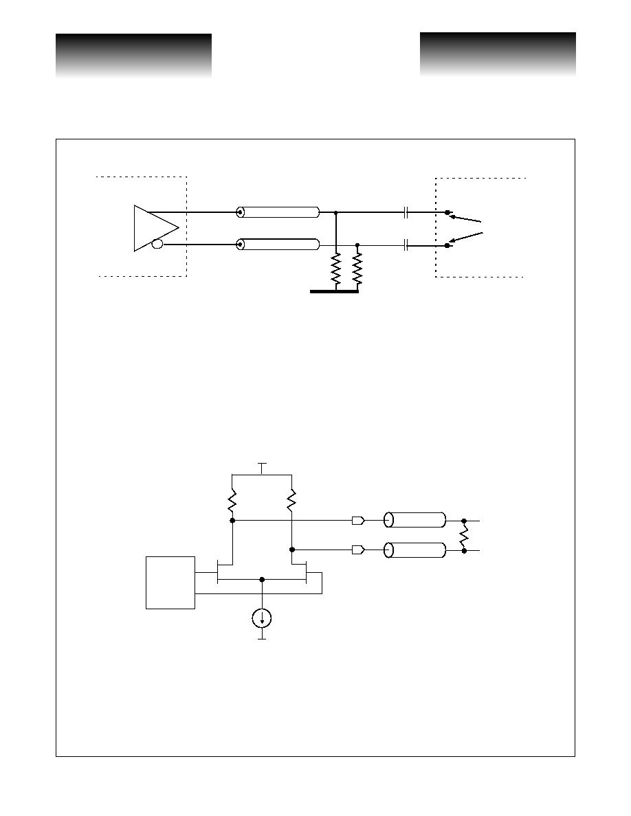
High-Speed Data and Clock Output
The high-speed data and clock output drivers consist of a differential pair designed to drive a 50
transmis-
sion line. The transmission line should be terminated with a 100
resistor at the load between true and comple-
ment outputs (see Figure 6). Connection to a termination voltage is not required. The output driver is back
terminated to 50
on-chip, providing a snubbing of any reflections. If used single-ended, the high-speed output
driver must still be terminated differentially at the load with a 100
resistor between true and complement out-
puts. The high-speed clock output can be powered down for additional power savings. To power down the high-
speed clock, tie the associated pins to V
CC
(see Table 3, Package Pin Identifications, pins 5,6,7).
Figure 6: High-Speed Output Termination
Clock Generator
An on-chip PLL generates the 2.48832GHz (or up to 2.7GHz for FEC) transmit clock from the externally
provided REFCLK input. The on-chip PLL uses a low phase noise reactance-based Voltage Controlled Oscilla-
tor (VCO) with an on-chip loop filter. The loop bandwidth of the PLL is within the SONET specified limit of
2MHz.
VSC8169
100nF
Z
o
Z
o
100nF
V
CC
-2V
downstream
bias point
generated
internally
50
50
V
CC
V
EE
Z
0
= 50
50
100
50
Pre-Driver
VITESSE
SEMICONDUCTOR CORPORATION
Preliminary Data Sheet
VSC8169
OC-48 (FEC) 16:1 SONET/SDH
MUX with Clock Generator
G52230-0, Rev 3.6
Page 5
01/02/01
© VITESSE
SEMICONDUCTOR CORPORATION ∑ 741 Calle Plano ∑ Camarillo, CA 93012
Tel: (800) VITESSE ∑ FAX: (805) 987-5896 ∑ Email: prodinfo@vitesse.com
Internet: www.vitesse.com
The customer can select to provide either a 77.76MHz (up to 84.38MHz- FEC) reference (recommended),
or the 2x of that reference, 155.52MHz (up to 168.75MHz-FEC). REF_FREQSEL is used to select the desired
reference frequency. REF_FREQSEL = "0" designates REFCLK
input
as 77.76MHz (up to 84.38MHz-FEC),
REF_FREQSEL = "1" designates REFCLK input as 155.52MHz (up to 168.75MHz - FEC) . For use with the
VSC9210 FEC Encoder/Decoder chipset running at 2.654208Gb/s, REF_FREQSEL = "0" should be selected
with the REFCLK
input
as 82.944MHz (serial rate divided by 32).
The REFCLK should be of high quality since noise on the REFCLK below the loop band width of the PLL
will pass through the PLL and appear as jitter on the output. Preconditioning of the REFCLK signal with a
VCXO may be required to avoid passing REFCLK noise with greater than 4ps RMS of jitter to the output. The
VSC8169 will output the REFCLK noise in addition to the intrinsic jitter from the VSC8169 itself during such
conditions.
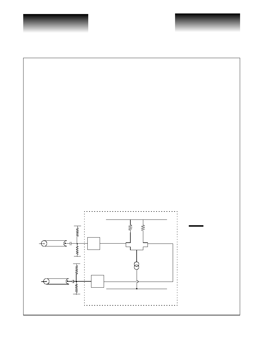
Low-Speed Inputs
The incoming low-speed data and reference clock input are received by LVPECL inputs D[15:0] and REF-
CLK. Off-chip termination of these inputs is required. For AC-coupling, a bias voltage suitable for AC-cou-
pling needs to be provided. See Figure 7 for external biasing resistor scheme..
In most situations these inputs will have high transition density and little DC offset. However, in cases
where this does not hold, direct DC connection is possible. All serial data inputs have the same circuit topology,
as shown in Figure 7. If the input signal is driven differentially and DC-coupled to the part, the mid-point of the
input signal swing should be centered about this common mode reference voltage (
V
CMI
)
and not exceed the
maximum allowable amplitude. For single-ended, DC-coupling operations, it is recommended that the user pro-
vides an external reference voltage. The external reference should have a nominal value equivalent to the com-
mon mode switch point of the DC-coupled signal, and can be connected to either side of the differential gate.
Figure 7: AC Termination of Low-Speed LVPECL REFCLK, D[15:0] Inputs
V
CC
= 3.3V
V
EE
= 0V
C
IN
Chip Boundary
Z
O
C
IN
TYP = 100nF
for AC operation
R2
R1
V
CC
V
EE
C
IN
Z
O
R2
R1
V
CC
V
EE
Split-end equivalent termination is Z
O
to V
TERM
R1 = 83
R2 = 125
, Zo=50
, V
TERM
= V
CC
-2V
V
CC
R2 + V
EE
R1
R1+R2
= V
Term
R1||R2 = Z
O