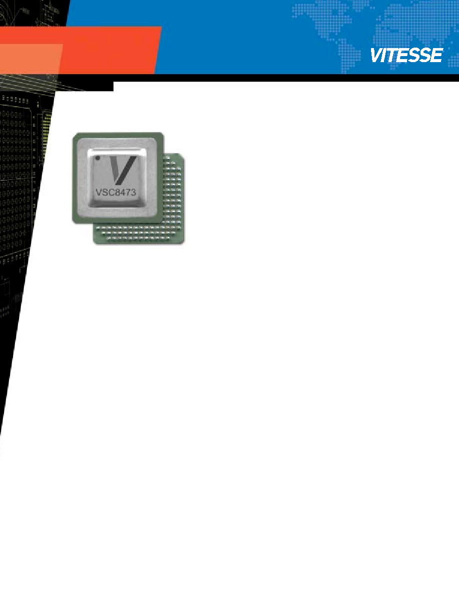
S P E C I F I C A T I O N S :
Frequency of Operation:
- VSC8473 9.95 Gb/s to 10.709 Gb/s
- VSC8473-01 9.95 Gb/s to 11.3 Gb/s
Exceeds SONET OC-192 Jitter Generation and Tolerance
Excellent Crosstalk Immunity and Asynchronous Tx and Rx operation
10mV Input Data Sensitivity (differential)
OIF 99.102.8 LVDS Compatible Parallel Data Inputs and Outputs
1.8V Single Power Supply with Optional 3.3V LVTTL I/O
1.15 Watt Typical Power
-5∫C Ambient to 90∫C Case Temperature
17mm x 17mm, 244-Ball, CBGA Package
A P P L I C A T I O N S :
300 pin MSA Transponder Modules
10GE and Fibre Channel to SFI-4 SERDES Applications
XFP Module XFI to Host SERDES Applications
DWDM and TDM SONET/SDH Line Cards
Add/Drop Mulitplexers
B E N E F I T S :
Low Power, Full Featured CMOS Transceiver
Single Chip Solution: Provides Complete Set of 300 pin MSA Transponder
Functions Including all Loopback and Clocking Modes
Robust Asynchronous Operation and High Immunity to Crosstalk
Multiple Reference Clock Source and Clean up Schemes
Pin Compatible Upgrade Path to VSC8477 with Phase Adjust and Sample
Optimizer Capability
F E A T U R E S :
16:1 Mux/Demux Transceiver With Integrated Clock Multiplier Unit,
and Clock and Data Recovery Unit with Limiting Amplifier
0.13
µm CMOS Process Technology
Full Support for 300-Pin MSA Transponder Modules:
- Multiple Reference Clock Source Inputs and Selectable Frequencies
- Programmable Transmit and Receive Multi-Rate Clock Outputs
- Facility and Equipment Loopback Modes
- Support for Line Timing Mode
- TxMClk, RxPOClk, RxMClk Support
- TxPClk with 0∫, 90∫, 180∫ and 270∫ Phase Adjustments
- Loss of Lock and FIFO Alarm Outputs
- Adjustable Loss of Signal Alarm
- Output Mutes
- CDR Lock to Reference Mode
I
2
C Micro-Controller Interface Port
- Programmable Registers for Access to All Control/Status Signals
TxRef Clock, RxRef Clock and ExRef Clock Sources
- Flexible Reference Clock Routing
- Reference Clock "Clean-up" Phase Detector
High-Speed Input Voltage Offset Adjust
High-Speed Data Inversion and Low-Speed Bit Order Swap
High-Speed CML Clock Output with Power Down Mode
9.953 to 10.709 Gb/s / 11.3 Gb/s SONET/SDH/10GE Transceiver with Integrated
Clock Generator and Clock Recovery
TRANSPORT PRODUCTS
PB-VSC8473-001
VSC8473

For more information on Vitesse Products visit the Vitesse web site
at www.vitesse.com or contact Vitesse Sales at (800) VITESSE
or sales@vitesse.com
©2003 Vitesse Semiconductor Corporation
9.953 to 10.709 Gb/s / 11.3 Gb/s SONET/SDH/10GE Transceiver with Integrated
Clock Generator and Clock Recovery
VSC8473
The VSC8473 is a 1:16 16:1 transceiver with
integrated Clock and Data Recovery unit
(CDR) and Clock Multiplier Unit (CMU), and
provides the most comprehensive solution
available for 300 pin module and DWDM
line card applications, with industry leading
optimization of power, performance, price and feature integration.
The 1.15 W total power dissipation enables module vendors to
provide performance and functionality advantages while dropping the
overall power dissipation of their existing modules. Full temperature
range and supply operation spans from 9.953 Gb/s to 10.709 Gb/s for
the VSC8473, and up to 11.3 Gb/s for the VSC8473-01. This provides
the most complete coverage in the industry of all operating rates
including SONET/SDH (9.95 Gb/s), 10GE (10.3 Gb/s), 10G Fibre
Channel (10.5 Gb/s), G.709 (10.7 Gb/s), 10GE+FEC (11.1 Gb/s) and
10G Fibre Channel + FEC (11.3 Gb/s.) The VSC8473 also provides an
excellent host SERDES capability for XFP module applications.
It fully supports all features, functions and clock modes required for
300-pin multi-source agreement (MSA) transponder module full
compliance. All loopback modes are supported with multiple line
timing clock modes. A highly flexible reference clock source selection
G E N E R A L D E S C R I P T I O N :
and reference clock clean-up support scheme is provided to minimize
external circuitry. An I
2
C serial interface provides full micro-controller
access to all status and control registers. Any combination of
discrete pins and serial register status and control can be employed.
Robust crosstalk immunity enables the VSC8473 to operate the Tx
and Rx paths asynchronously to each other while exceeding SONET
level jitter generation and jitter tolerance performance. A high-
speed output clock can be optionally enabled for higher
performance applications. An adjustable loss of signal (LOS)
indicator is integrated into the device enabling optical modulation
amplitude monitoring.
The power supply scheme provides a high degree of flexibility. It can
operate on a single +1.8V supply with an optional +3.3V I/O supply
for interfacing. The single chip, small footprint (17 x 17 mm) design
allows for both cost reduction and board size reduction for price-
and-size aggressive, small form factor module applications. A pin-
compatible VSC8477 device provides additional functions including
full data eye phase and threshold adjust, sample optimization and
data eye mapping capabilities. All VSC8473/77 devices are tested
at high-speed to ensure the highest performance and quality
standards you've come to expect from Vitesse.
741 Calle Plano
Camarillo, CA 93012, USA
Tel: +1 805.388.3700
Fax: +1 805.987.5896
www.vitesse.com
V S C 8 4 7 3 B L O C K D I A G R A M :
1:16
DEMUX
CMU
CDR
Test
RxPOClk
Line Loopback
16:1
MUX
Low-Speed Data
TxPIClk
High-Speed Data
Tx Ref Clock
Diagnostic Loopback
High-Speed Data
High-Speed Clock*
16 Low-Speed Data
TxMClk
I
2
C
Interface
Control/Status Signals
I
2
C Port
16
LA
SFI-4
Phase 1/
XSBI
SFI-4
Phase 1/
XSBI
FIFO
16x16
Reference Clk
Distribution and
Clean Up
Support
Rx Ref Clock
Ex Ref Clock
* With Enable/Disable
Adjustable LOS
FIFO Alarm
TxPClk w/Phs Adj
Mute Controls
Invert Controls
LOL Alarms
RxMClk

