
Document:1G5-0160
Rev.1
Page 1
VIS
Preliminary VG3617161DT
16Mb CMOS Synchronous Dynamic RAM
Description
The VG3617161DT is CMOS Synchronous Dynamic RAM organized as 524,288-word X 16-bit X 2-bank.
It is fabricated with an advanced submicron CMOS technology and designed to operate from a single 3.3V
power supply. This SDRAM is delicately designed with performance concern for current high-speed applica-
tion. Programmable CAS Latency and Burst Length make it possible to be used in widely various domains. It
is packaged by using JEDEC standard pinouts and standard plastic 50-pin TSOP II.
Features
∑ Single 3.3V +/- 0.3V power supply
∑ Clock Frequency: 180MHz, 166MHz, 143MHz, 125MHz, 100MHz
∑ Fully synchronous with all signals referenced to a positive clock edge
∑ Programmable CAS Iatency (2,3)
∑ Programmable burst length (1,2,4,8,& Full page)
∑ Programmable wrap sequence (Sequential/Interleave)
∑ Automatic precharge and controlled precharge
∑ Auto refresh and self refresh modes
∑ Dual internal banks controlled by A11(Bank select)
∑ Simultaneous and independent two bank operation
∑ I/O level : LVTTL interface
∑ Random column access in every cycle
∑ X16 organization
∑ Byte control by LDQM and UDQM
∑ 4096 refresh cycles/64ms
∑ Burst termination by burst stop and precharge command
Document:1G5-0160
Rev.1
Page 2
VIS
Preliminary VG3617161DT
16Mb CMOS Synchronous Dynamic RAM
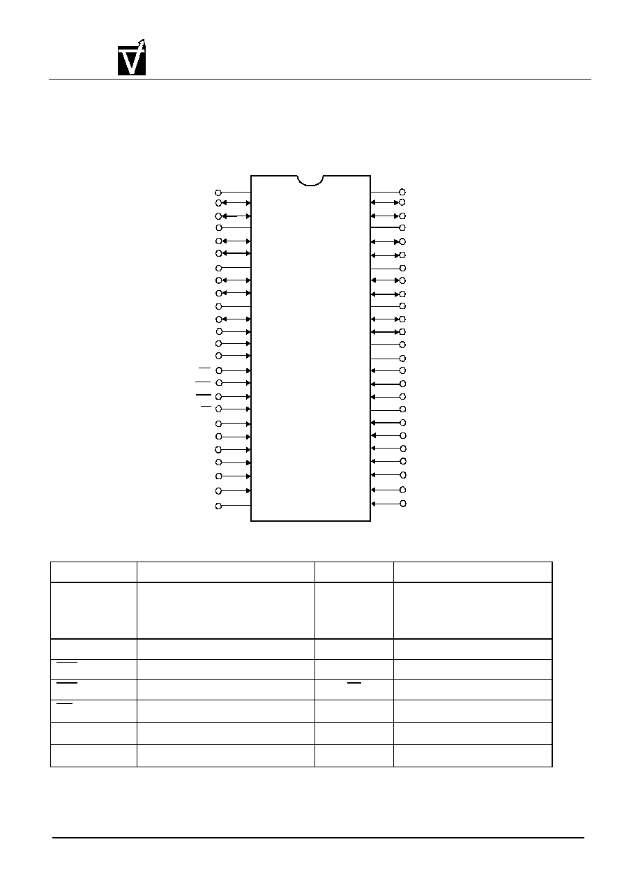
Pin Configuration
Pin Description
(VG3617161DT)
Pin Name
Function
Pin Name
Function
A0-A11
Address inputs
- Row address A0-A10
- Column address A0-A8
A11: Bank select
LDQM,
UDQM
Lower DQ mask enable and
Upper DQ mark enable
DQ0~DQ15
Data-in/data-out
CLK
Clock input
RAS
Row address strobe
CKE
Clock enable
CAS
Column address strobe
CS
Chip select
WE
Write enable
V
DDQ
Supply voltage for DQ
V
SS
Ground
V
SSQ
Ground for DQ
V
DD
Power
1
2
3
4
5
6
7
8
9
10
11
12
13
14
15
16
17
18
19
20
21
22
44
43
42
41
38
37
36
35
34
33
32
31
30
29
28
27
26
V
G
3
6
1
7
1
6
1
D
T
50-Pin Plastic TSOP(II)(400 mil)
V
DD
DQ0
V
DDQ
DQ1
V
SSQ
DQ2
DQ3
DQ4
V
SSQ
CAS
A
10
(BS)A
11
A
0
A
1
V
SS
DQ15
V
SSQ
DQ13
V
SSQ
DQ12
V
DDQ
DQ11
CLK
DQ8
NC
UDQM
CKE
NC
A8
A9
A7
A6
DQ5
DQ6
DQ7
V
DDQ
23
24
25
50
49
48
47
46
45
DQ14
DQ10
DQ9
V
DDQ
A5
A4
V
SS
A
2
A
3
V
DD
CS
40
39
LDQM
RAS
WE
Document:1G5-0160
Rev.1
Page 3
VIS
Preliminary VG3617161DT
16Mb CMOS Synchronous Dynamic RAM
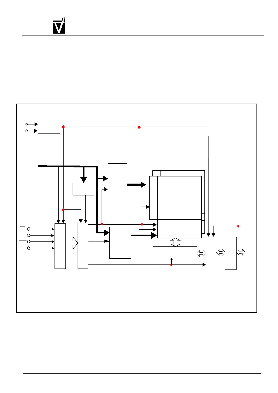
Block Diagram
CLK
CKE
Clock
Generator
CS
RAS
Mode
Register
Column
Address
Buffer
&
Burst
Counter
CAS
WE
C
o
m
m
a
n
d
D
e
c
o
d
e
r
C
o
n
t
r
o
l
L
o
g
i
c
Address
Row
Address
Buffer
&
Refresh
Counter
Bank B
Bank A
Sense Amplifier
Column Decoder &
Latch Circuit
R
o
w
D
e
c
o
d
e
r
Data Control Circuit
DQ
DQM
L
a
t
c
h
C
i
r
c
u
i
t
I
n
p
u
t
&
O
u
t
p
u
t
B
u
f
f
e
r
Document:1G5-0160
Rev.1
Page 4
VIS
Preliminary VG3617161DT
16Mb CMOS Synchronous Dynamic RAM
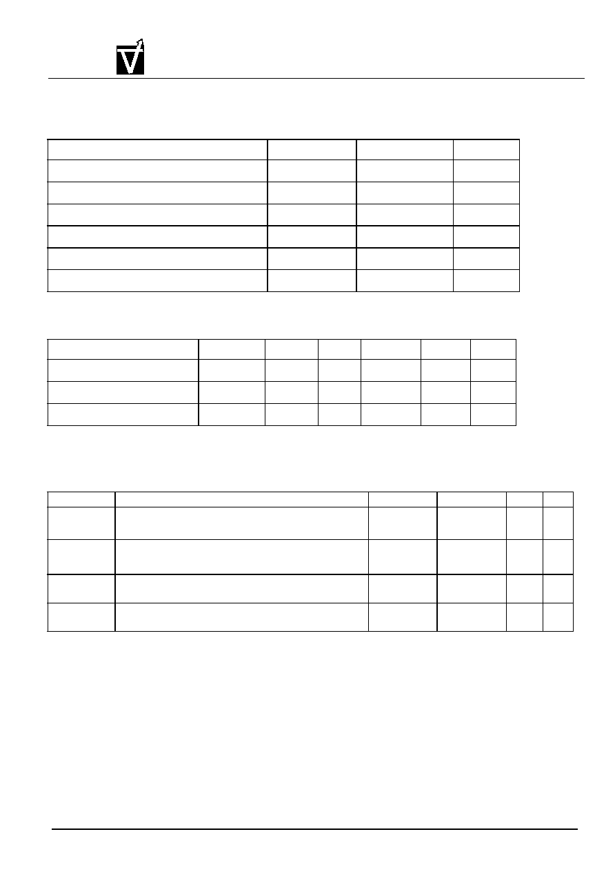
Absolute Maximum Ratings
Recommended DC Operating Conditions
Note 1.Overshoot limit : V
IH(MAX.)
=V
DDQ
+2.0V with a pulse width < 3ns
2.Undershoot limit : V
IL
=V
SSQ
-2.0V with a pulse < 3ns and -1.5V with a pulse < 5ns
Parameter
Symbol
Value
Unit
Voltage on any pin relative to Vss
V
IN
,V
OUT
-1.0 to +4.6
V
Supply voltage relative to Vss
V
DD
,V
DDQ
-1.0 to +4.6
V
Short circuit output current
I
OUT
50
mA
Power dissipation
P
D
1.0
W
Operating temperature
T
OPT
0 to + 70
¢
J
Storage temperature
T
STG
-55 to + 125
¢
J
Parameter
Symbol
Min
Typ
Max
Unit
Note
Supply Voltage
V
DD
3.0
3.3
3.6
V
Input High Voltage, all inputs
V
IH
2.0
°
–
V
DD
+0.3
V
1
Input Low Voltage, all inputs
V
IL
-0.3
°
–
0.8
V
2
Parameter
Description
Min.
Max.
Unit
Note
I
IL
Input Leakage Current
(
All other pins not under test = OV)
-5
5
A
I
OL
Output Leakage Current
Output disable, (
)
-5
5
A
V
OH
LVTTL Output "H" Level Voltage
(l
OUT
= -2mA)
2.4
-
V
V
OL
LVTTL Output "L" Level Voltage
(l
OUT
= 2mA)
-
0.4
V
0V
V
IN
V
DD
µ
0V
V
OUT
V
DDQ
µ

Document:1G5-0160
Rev.1
Page 5
VIS
Preliminary VG3617161DT
16Mb CMOS Synchronous Dynamic RAM
Capacitance
(Ta=25∞C,f=1MHZ)
Recommended D.C. Operating Conditions (V
DD
= 3.3V 0.3V, Ta = 0 ~ 70∞C)
Parameter
Symbol
Typ
Max
Unit
Input capacitance(CLK)
C
11
2.5
4
pF
Input capacitance(all input pins except data
pins)
C
12
2.5
5
pF
Data input/output capacitance
C
I/O
4.0
6.5
pF
Description/test condition
Symbol
-5.5
-6
-7
-8
Unit
Note
Min. Max. Min. Max. Min. Max. Min. Max.
Operating Current
, Outputs Open
Address changed once during t
CK(min)
.
Burst Length = 1 (One Bank Active)
I
DD1
190
185
165
145
mA
3,4
Precharge Standby Current in non power-down mode
t
CK
= t
CK(min)
,
(min)
,
(min)
Input signals are changed once during 30ns.
I
DD2N
95
85
75
65
3
Precharge Standby Current in non power-down mode
t
CK
= ,
(min)
,
(max)
Input signals are stable
I
DD2NS
45
40
35
30
Precharge Standby Current in power-down mode
t
CK
= t
CK
(min),
(max)
I
DD2P
4
4
4
4
3
Precharge Standby Current in power-down mode
t
CK
= ,
(max)
,
(max)
I
DD2PS
3.5
3.5
3.5
3.5
Active Standby Current in non power down mode
(min)
, t
CK
= t
CK(min)
(Both Bank Actioe)
I
DD3N
85
75
65
55
3
Active Standby Current in power-down
(max)
, t
CK =
t
CK(min)
, CS
V
IH(min)
(Both
Bank Active)
I
DD3P
6
6
6
6
Operating Current (Page Burst, and All Bank activated)
t
CCD
= t
CCD(min)
, Outputs Open, Multi-bank interleave,
gapless data
I
DD4
195
185
175
165
4,5
Refresh Current
(min)
(t
REF
= 64ms)
I
DD5
185
175
165
155
3
Self Refresh Current
I
DD6
4
4
4
4
±
t
R C
t
RC min
(
)
C S
V
I H
CKE
V
I H
CKE
V
I H
CLK
V
IL
CKE
V
I L
CKE
V
I L
CLK
V
IL
CKE
V
I H
CKE
V
I L
t
RC
t
RC
CKE
0.2V