
Document : 1G5-0099
Rev.1
Page 1
VIS
Preliminary VG3664321(4)1(2)BT
CMOS Synchronous Dynamic RAM
Description
The device is CMOS Synchronous Dynamic RAM organized as 524,288 - word x 32 - bit x 4 -
bank, and 1,048,576 - word x 32 - bit x 2 - bank, respectively. lt is fabricated with an advanced
submicron CMOS technology and designed to operate from a singly 3.3V only power supply. It is
packaged in JEDEC standard pinout and standard plastic TSOP package.
Features
∑ Single 3.3V (
) power supply
∑ High speed clock cycle time : 8/10 for LVTTL
∑ High speed clock cycle time : 8/10 for SSTL - 3
∑ Fully synchronous with all signals referenced to a positive clock edge
∑ Programmable CAS Iatency (2,3)
∑ Programmable burst length (1,2,4,8,& Full page)
∑ Programmable wrap sequence (Sequential/Interleave)
∑ Automatic precharge and controlled precharge
∑ Auto refresh and self refresh modes
∑ Dual Internal banks controlled by A11 (Bank select) for VG36643211(2)
∑ Quad Internal banks controlled by A11 & A12 (Bank select) for VG36643241(2)
∑ Each Banks can operate simultaneously and independently
∑ LVTTL compatible I/O interface for VG36643211 and VG36643241
∑ SSTL - 3 compatible I/O interface for VG36643212 and VG36643242
∑ Random column access in every cycle
∑ x32 organization
∑ Input/Output controlled by DQM0 ~ 3
∑ 4,096 refresh cycles/64ms
∑ Burst termination by burst stop and precharge command
∑ Burst read/single write option
0.3V
±
Document : 1G5-0099
Rev.1
Page 2
VIS
Preliminary VG3664321(4)1(2)BT
CMOS Synchronous Dynamic RAM
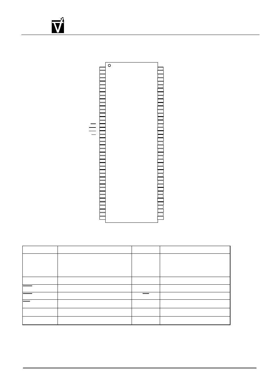
Pin Configuration
Pin Description
VG36643211 (2)
Pin Name
Function
Pin Name
Function
A0 - A11
Address inputs
- Row address A0 - A10
- Column address A0 - A8
A11 : Bank select
DQM0 ~ 3
DQ Mask enable
DQ0 ~ DQ31
Data - in/data - out
CLK
Clock input
RAS
Row address strobe
CKE
Clock enable
CAS
Column address strobe
CS
Chip select
WE
Write enable
V
DDQ
Supply voltage for DQ
V
SS
Ground
V
SSQ
Ground for DQ
V
DD
Power ( + 3.3V)
(V
REF
)
Reference Voltage, SSTL - 3 only
1
2
3
4
5
6
7
8
9
10
11
12
13
14
15
16
17
18
19
20
21
22
23
24
25
26
27
28
29
30
31
32
33
34
35
36
37
38
39
40
41
42
43
86
85
84
83
82
81
80
79
78
77
76
75
73
72
71
70
69
68
67
66
65
64
63
62
61
60
59
58
57
56
55
54
53
52
51
50
49
48
47
46
45
44
74
V
DD
DQ0
V
DDQ
DQ1
DQ2
V
SSQ
DQ3
DQ4
V
DDQ
DQ5
DQ6
V
SSQ
DQ7
NC
V
DD
DQM0
WE
CAS
RAS
CS
NC
A11/BA
NC
A10/AP
A0
A1
A2
DQM2
V
DD
NC
DQ16
V
SSQ
DQ17
DQ18
V
DDQ
DQ19
DQ20
V
SSQ
DQ21
DQ22
V
DDQ
DQ23
V
DD
V
SS
DQ15
V
SSQ
DQ14
DQ13
V
DDQ
DQ11
DQ12
V
SSQ
DQ10
DQ9
V
DDQ
DQ8
NC
V
SS
DQM1
NC (VREF)
NC
CLK
CKE
A9
A8
A7
A6
A5
A4
A3
DQM3
V
SS
NC
DQ31
V
DDQ
DQ30
DQ29
V
SSQ
DQ28
DQ27
V
DDQ
DQ26
DQ25
V
SSQ
DQ24
V
SS
Document : 1G5-0099
Rev.1
Page 3
VIS
Preliminary VG3664321(4)1(2)BT
CMOS Synchronous Dynamic RAM
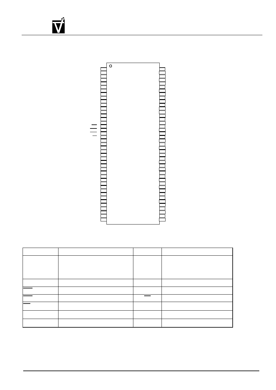
Pin Configuration
Pin Description
VG36643241 (2)
Pin Name
Function
Pin Name
Function
A0 - A12
Address inputs
- Row address A0 - A10
- Column address A0 - A7
A11 & A12 : Bank select
DQM0 ~ 3
DQ Mask enable
DQ0 ~ DQ31
Data - in/data - out
CLK
Clock input
RAS
Row address strobe
CKE
Clock enable
CAS
Column address strobe
CS
Chip select
WE
Write enable
V
DDQ
Supply voltage for DQ
V
SS
Ground
V
SSQ
Ground for DQ
V
DD
Power ( + 3.3V)
(V
REF
)
Reference Voltage, SSTL - 3 only
1
2
3
4
5
6
7
8
9
10
11
12
13
14
15
16
17
18
19
20
21
22
23
24
25
26
27
28
29
30
31
32
33
34
35
36
37
38
39
40
41
42
43
86
85
84
83
82
81
80
79
78
77
76
75
73
72
71
70
69
68
67
66
65
64
63
62
61
60
59
58
57
56
55
54
53
52
51
50
49
48
47
46
45
44
74
V
DD
DQ0
V
DDQ
DQ1
DQ2
V
SSQ
DQ3
DQ4
V
DDQ
DQ5
DQ6
V
SSQ
DQ7
NC
V
DD
DQM0
WE
CAS
RAS
CS
NC
A12/BA0
A10/AP
A0
A1
A2
DQM2
V
DD
NC
DQ16
V
SSQ
DQ17
DQ18
V
DDQ
DQ19
DQ20
V
SSQ
DQ21
DQ22
V
DDQ
DQ23
V
DD
V
SS
DQ15
V
SSQ
DQ14
DQ13
V
DDQ
DQ11
DQ12
V
SSQ
DQ10
DQ9
V
DDQ
DQ8
NC
V
SS
DQM1
NC (VREF)
NC
CLK
CKE
A9
A8
A7
A6
A5
A4
A3
DQM3
V
SS
NC
DQ31
V
DDQ
DQ30
DQ29
V
SSQ
DQ28
DQ27
V
DDQ
DQ26
DQ25
V
SSQ
DQ24
V
SS
A11/BA1
Document : 1G5-0099
Rev.1
Page 4
VIS
Preliminary VG3664321(4)1(2)BT
CMOS Synchronous Dynamic RAM
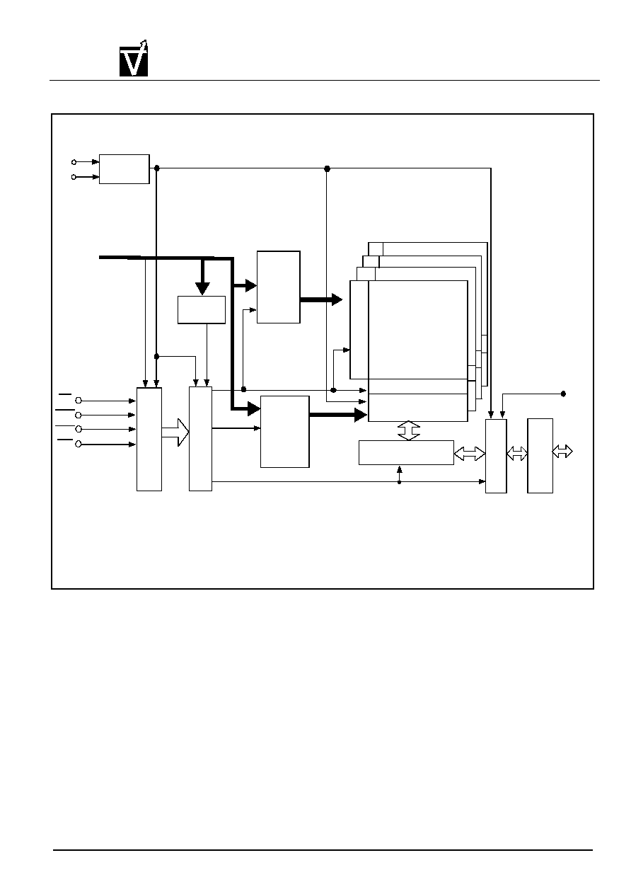
Block Diagram
CLK
CKE
Clock
Generator
CS
RAS
Mode
Register
Column
Address
Buffer
&
Burst
Counter
CAS
WE
C
o
m
m
a
n
d
D
e
c
o
d
e
r
C
o
n
t
r
o
l
L
o
g
i
c
Address
Row
Address
Buffer
&
Refresh
Counter
Bank B
Bank A
Sense Amplifier
Column Decoder &
Latch Circuit
R
o
w
D
e
c
o
d
e
r
Data Control Circuit
DQ
DQM
L
a
t
c
h
C
i
r
c
u
i
t
I
n
p
u
t
&
O
u
t
p
u
t
B
u
f
f
e
r
(Bank C)
(Bank D)
Note: Bank C and Bank D are for VG36643241(2) only
Document : 1G5-0099
Rev.1
Page 5
VIS
Preliminary VG3664321(4)1(2)BT
CMOS Synchronous Dynamic RAM
Absolute Maximum D.C. Ratings
Caution Exposing the device to stress above those listed in Absolute Maximum Ratings could cause
permanent damage. The device is not meant to be operated under conditions outside the limits
described in the operational section of this specification. Exposure to Absolute Maximum Rating
conditions for extended periods may affect device reliability.
Parameter
Symbol
Value
Unit
Voltage on any pin relative to Vss
V
IN
, V
OUT
-0.5 to + 4.6
V
Supply voltage relative to Vss
V
DD
, V
DDQ
-0.5 to + 4.6
V
Short circuit output current
I
OUT
50
mA
Power dissipation
P
D
1.0
W
Operating temperature
T
OPT
0 to + 70
∞C
Storage temperature
T
STG
-55 to + 125
∞C
Maximum A.C. Operating Requirements for LVTTL Compatible
Parameter
Symbol
Min
Max
Unit
Notes
Input High Voltage
V
IH
2.0
V
DDQ
+ 2.0
V
2
Input Low Voltage
V
IL
V
SSQ
-2.0
0.8
V
2
Recommended DC Operating Conditions for LVTTL Compatible
Parameter
Symbol
Min
Typ
Max
Unit
Supply Voltage
V
DD,
V
DDQ
3.0
3.3
3.6
V
Input High Voltage, all inputs
V
IH
2.0
-
V
DD
+ 0.3
V
Input Low Voltage, all inputs
V
IL
-0.3
-
0.8
V
Recommended DC Operating Conditions for SSTL - 3 Interface
Parameter
Symbol
Min
Typ
Max
Unit
Supply Voltage
V
DD,
V
DDQ
3.0
3.3
3.6
V
Supply Voltage (Ground)
V
SS,
V
SSQ
0
-
0
V
Reference Voltage
V
REF
1.3
1.5
1.7
V
Termination Voltage
V
TT
V
REF
-005
V
REF
V
REF
+ 0.05
V
Input High Voltage, all inputs
V
IH(dc)
V
REF
+ 0.2
-
V
DD
+ 0.3
V
Input Low Voltage, all inputs
V
IH(dc)
-0.3
-
V
REF
-0.2
V
Capacitance
(Ta = 25∞C, f = 1MHZ)
Notes : 1. Capacitance measured with effective capacitance measuring method.
2. The overshoot and undershoot voltage duration is
3ns with no input clamp diodes.
Parameter
Symbol
Typ
Max
Unit
Notes
Input capacitance (Address)
C
I1
-
4
pF
1
Input capacitance (all input pins
except address pins & data pins.)
C
I2
-
4
pF
1
Data input/output capacitance
C
I/O
-
5
pF
1