Document : 1G5-0193
Rev.1
Page 1
VIS
VG37256402AT
VG37256802AT
CMOS DDR Synchronous Dynamic RAM
Description
The 256Mb DDR SDRAM is a high-speed COMS, dynamic random-access memory con-
taining 268,435,456 bits. It is internally configured as a quad-bank DRAM. The 256Mb DDR
SDRAM uses a double-data-rate architecture to achieve high-speed operation. A bidirec-
tional data strobe (DQS) is transmitted externally, along with data, for use in data capture at
the receiver. DQS is an intermittent strobe transmitted by the DDR SDRAM during READs
and by the memory controller during WRITEs. DQS is edge-aligned with data for READs and
center-aligned with data for WRITEs.
The 256Mb DDR SDRAM operates from a differential clock (CLK and CLK#; the crossing
of CLK going HIGH and CLK# going LOW will be referred to as the positive edge of CLK).
Commands (address and control signals) are registered at every positive edge of CLK. Input
data is latched by both edges of DQS with DQS aligned to center of data packet, and output
data is latched by both edges of DQS with DQS aligned to edge of data packet.
The DDR SDRAM provides for programmable READ or WRITE burst lengths of 2, 4 or 8
locations. An AUTO PRECHARGE function may be enabled to provide a self-timed row pre-
charge that is initiated at the end of the burst access.
As with standard SDRAMs, the pipelined, multibank architecture of DDR SDRAMs allows
for concurrent operation, thereby providing high effective bandwidth by hiding row precharge
and activation time.
The 256Mb DDR SDRAM is designed to operate in either low-power memory systems.
An auto refresh mode is provided, along with a power-saving, power-down mode. All inputs
are compatible with the JEDEC Standard for SSTL_2. All outputs are SSTL_2, Class II com-
patible.
Note: The functionality described in, and the timing specifications included in this data sheet
are for the DLL Enabled mode of operation. This is the only normal operating mode for these
DDR devices.
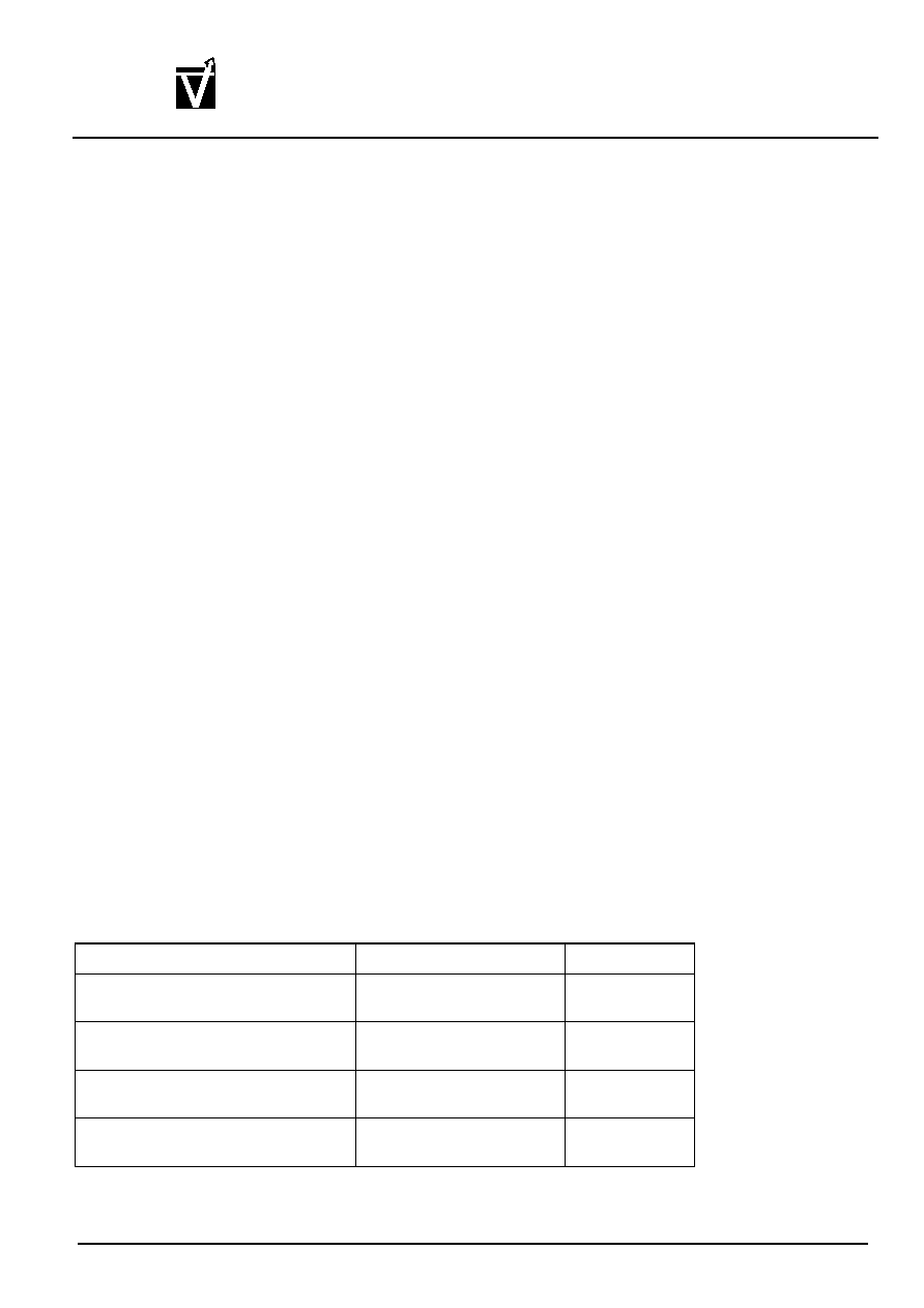
Operating Frequencies
Part Number
Cycle time
Standard
VG3725640(80)2AT-66
6.6 ns (150MHz CL=2.5)
7.5 ns (133MHz CL=2)
DDR300
VG3725640(80)2AT-7L
7.5 ns (133MHz CL=2)
7.5 ns (133MHz CL=2.5)
DDR266A
VG3725640(80)2AT-75
7.5 ns (133MHz CL=2.5)
10 ns (100MHz CL=2)
DDR266B
VG3725640(80)2AT-8
8 ns (125MHz CL=2.5)
10 ns (100MHz CL=2)
DDR200

Document : 1G5-0193
Rev.1
Page 2
VIS
VG37256402AT
VG37256802AT
CMOS DDR Synchronous Dynamic RAM
Features
∑
JEDEC standard
∑
Double-data-rate architecture: two data transfers per clock cycle
∑
Bidirectional, intermittent data strobe (DQS) is transmitted/received with data, to be used in
capturing data at the receiver
∑
DQS is edge-aligned with data for READs, and center-aligned with data for WRITEs
∑
Differential clock inputs (CLK and CLK#)
∑
DLL aligns DQ and DQS transitions with CLK transitions
∑
Commands entered on each positive CLK edge; data and data mask referenced to both edges of DQS
∑
Four internal banks for concurrent operation
∑
Data mask (DM) for write data
∑
Burst lengths: 2, 4, or 8 (programmable)
∑
CAS Latency: 2, 2.5 (programmable)
∑
Burst type: sequential / interleave (programmable)
∑
AUTO PRECHARGE / All bank precharge controlled by A10
∑
Auto Refresh and Self Refresh Modes
∑
8192 refresh cycles / 64ms (4 banks concurrent refresh)
∑
2.5V (SSTL_2 compatible) I/O
∑
400-mil, 66-pin TSOP II

Document : 1G5-0193
Rev.1
Page 3
VIS
VG37256402AT
VG37256802AT
CMOS DDR Synchronous Dynamic RAM
Column Address Table
Organization
Column Address
32Mx8
A0-A9
64Mx4
A0-A9, A11
32M X 8
V
DD
DQ0
V
DDQ
DQ2
NC
NC
DQ1
NC
DQ3
NC
64M X 4
P
in Configuration
1
2
3
4
5
6
7
8
9
10
11
12
13
14
16
17
18
19
20
21
22
56
55
54
23
24
25
26
27
41
40
43
42
48
47
46
45
44
50
49
51
52
53
58
57
59
60
61
62
63
64
65
66
15
28
39
29
38
30
31
32
33
37
36
35
34
256M DDR SDRAM (x4/x8) Pin-out
V
DD
NC
V
DDQ
NC
CAS
RAS
WE
NC
DQ0
NC
DQ1
NC
NC
CS
BA1
BA0
V
DD
NC
NC
A
0
A
1
A
3
V
DD
V
DDQ
NC
A
10
/AP
A
2
NC
NC
NC
V
DD
NC
CAS
RAS
WE
CS
BA1
BA0
NC
NC
A
0
A
1
A
3
V
DD
A
10
/AP
A
2
V
SS
V
SSQ
V
DDQ
DQ5
DQ4
V
DDQ
NC
V
SS
A
9
A
8
A
7
A
6
A
5
A
12
A
4
V
SSQ
DQ6
DQ7
NC
NC
NC
NC
NC
V
SSQ
DQS
NC
V
REF
V
SS
DM
CK
CK
CKE
A
11
V
SS
V
SSQ
V
DDQ
NC
DQ2
V
DDQ
V
SS
A
9
A
8
A
7
A
6
A
5
A
12
A
4
V
SSQ
DQ3
NC
NC
NC
NC
NC
NC
V
SSQ
DQS
NC
V
REF
V
SS
DM
CK
CK
CKE
A
11
Top View
66 PIN TSOP(II)
(400 mil x 875 mil)
(0.65 mm PIN PITCH)
Bank Address:
BA0-BA1
Row Address:
A0-A12
Auto Precharge:
A10
NC
V
SSQ
V
DDQ
V
SSQ
V
DDQ
V
SSQ
NC
V
DDQ
V
SSQ
NC
NC

Document : 1G5-0193
Rev.1
Page 4
VIS
VG37256402AT
VG37256802AT
CMOS DDR Synchronous Dynamic RAM
DLL
I/O B
UFFER
DQS B
UFFER
DQ0-DQ7
DQS
M
EMORRY
A
RRAR
B
ANK
0
M
EMORRY
A
RRAR
B
ANK
3
M
EMORRY
A
RRAR
B
ANK
2
M
EMORRY
A
RRAR
B
ANK
1
M
ODE
R
EGISTER
C
ONTROL
C
IRCUITRY
A
DDRESS
B
UFFER
C
LOCK
B
UFFER
C
ONTROL
S
IGNAL
B
UFFER
A0-12 BA0, 1
CLK, /CLK CKE
/CS /RAS /CAS /WE DM
FUNCTIONAL BLOCK DIAGRAM
Note 1: This Functional Block Diagram is intended to facilitate user understanding of the operation of the
device; it does not necessarily represent an actual circuit implementation.
Note 2: DM is a unidirectional signal (input only) but is internally loaded to match the load of the bidirectional
DQ and DQS signals.

Document : 1G5-0193
Rev.1
Page 5
VIS
VG37256402AT
VG37256802AT
CMOS DDR Synchronous Dynamic RAM
PIN DESCRIPTIONS
Symbol
Type
Description
CLK,CLK#
Input
Clock: CLK and CLK# are differential clock inputs. All address and control input sig-
nals are sampled on the positive edge of CLK (negative edge of CLK#). Output (read)
data is referenced to both edges of CLK. Internal clock signals are derived from CLK/
CLK#.
CKE
Input
Clock Enable: CKE HIGH activates, and CKE LOW deactivates internal clock sig-
nals, device input buffers and output drivers. Deactivating the clock provides PRE-
CHARGE POWER-DOWN and SELF REFRESH operation (all banks idle), or
ACTIVE POWER-DOWN (row ACTIVE in any bank). CKE is synchronous for all
functions except for disabling outputs, which is achieved asynchronously. Input buff-
ers, excluding CLK, CLK# and CKE are disabled during power-down and self refresh
modes, providing low standby power. CKE will recognize an LVCMOS LOW level
prior to VREF being stable on power-up.
CS#
Input
Chip Select: CS# enables (registered LOW) and disables (registered HIGH) the com-
mand decoder. All commands are masked when CS# is registered HIGH. CS# pro-
vides for external bank selection on systems with multiple banks. CS# is considered
part of the command code.
RAS#,CAS#,
WE#
Input
Command Inputs: RAS#, CAS# and WE# (along with CS#) define the command
being entered.
DM
Input
Input Data Mask: DM is an input mask signal for write data. Input data is masked
when DM is sampled HIGH along with that input data during a WRITE access. DM is
sampled on both edges of DQS. DM pins include dummy loading internally, to match
the DQ and DQS loading.
BA0,BA1
Input
Bank Address Inputs: BA0 and BA1 define to which bank an ACTIVE, READ, WRITE
or PRECHARGE command is being applied.
A0-A12
Input
Address Inputs: Provide the row address for ACTIVE commands and the column
address and AUTO PRECHARGE bit for READ/WRITE commands, to select one
location out of the memory array in the respective bank. A10 is sampled during a
PRECHARGE command to determine whether the PRECHARGE applies to one
bank (A10 LOW) or all banks (A10 HIGH). If only one bank is to be precharged, the
bank is selected by BA0,BA1. The address inputs also provide the op-code during a
MODE REGISTER SET command.
DQ
I/O
Data Input/Output: Data bus
DQS
I/O
Data Strobe: Output with read data, input with write data. Edge-aligned with read
data, centered in write data. Used to capture write data.
NC
-
No Connect: these pins should be left unconnected.
V
DDQ
Supply
DQ Power Supply:+2.5V
.
V
SSQ
Supply
DQ Ground.
V
DD
Supply
Power Supply: +2.5V
.
V
SS
Supply
Ground.
V
REF
Input
SSTL_2 reference voltage.
0.2V
±
0.2V
±