
Document:1G5-0185
Rev.1
Page 1
VIS
VS864648041D,VS1664648041D
8M,16MX64-Bit
SDRAM Module
Description
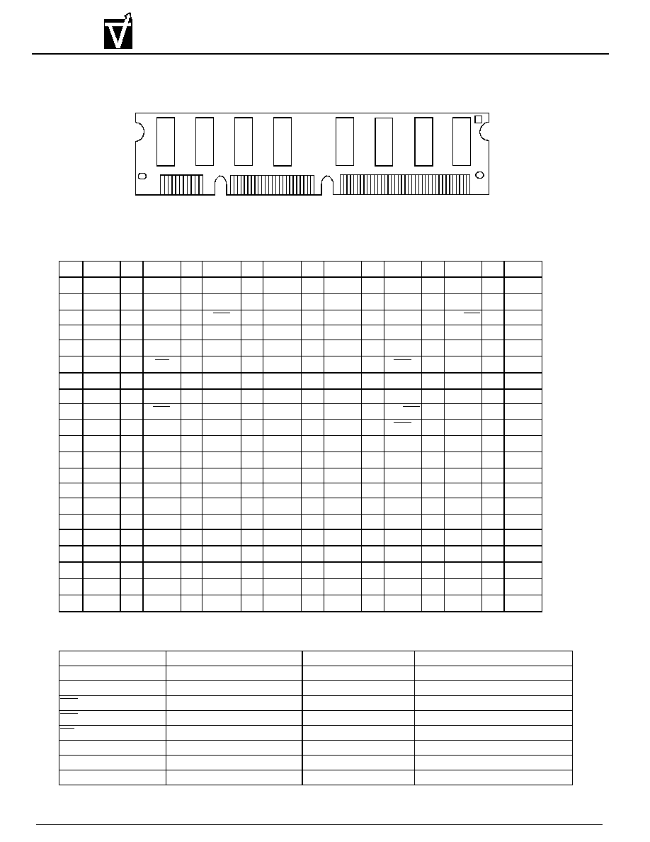
The VS864648041D and VS1664648041D are 8M x 64 bit and 16M bit x 64 Dual-In-Line synchronous
DRAM Module (DIMM). It consists of 8/16 CMOS 8Mx8 bit synchronous DRAMs (VG36648041DT) with 4
banks and in standard 54 pin TSOP-II package. Decoupling capacitors are mounted on power supply line for
noise reduction. The module use serial presence detects implemented via a 2K-bit EEPROM component.
Features
VS864648041D, VS1664648041D :
∑ Comply to Intel PC100/JEDEC PC133 specification
∑ Single 3.3V (
) power supply
∑ Utilizes -7, -7L and -8H SDRAM components
∑ 8M x 64 bit (VS864648041D) and 16M x 64 bit (VS1664648041D) options
∑ Fully synchronous with all signals referenced to a positive clock edge
∑ Non-Buffered
∑ Programmable burst length (1,2,4,8 & Full page)
∑ Programmable wrap sequence (Sequential/Interleave)
∑ Automatic precharge and controlled precharge
∑ Auto refresh and self refresh modes
∑ I/O level : LVTTL interface
∑ Random column access in every cycle
∑ 4096 refresh cycles / 64ms
∑ Serial Presence Detect (SPD) with EEPROM
∑ JEDEC standard pinout
0.3V
±
Document:1G5-0185
Rev.1
Page 2
VIS
VS864648041D,VS1664648041D
8M,16MX64-Bit
SDRAM Module
Pin Configurations
*
16M x 64 version only
Pin Description
Pin
Name
Pin
Name
Pin
Name
Pin
Name
Pin
Name
Pin
Name
Pin
Name
Pin
Name
1
V
SS
22
NC
43
V
SS
64
V
SS
85
V
SS
106
NC
127
V
SS
148
V
SS
2
DQ0
23
V
SS
44
NC
65
DQ21
86
DQ32
107
V
SS
128
CKE0
149
DQ53
3
DQ1
24
NC
45
CS2
66
DQ22
87
DQ33
108
NC
129 NC\*CS3 150
DQ54
4
DQ2
25
NC
46
DQMB2
67
DQ23
88
DQ34
109
NC
130
DQMB6
151
DQ55
5
DQ3
26
V
DD
47
DQMB3
68
V
SS
89
DQ35
110
V
DD
131
DQMB7
152
V
SS
6
V
DD
27
WE
48
NC
69
DQ24
90
V
DD
111
CAS
132 NC\*A13 153
DQ56
7
DQ4
28
DQMB0
49
V
DD
70
DQ25
91
DQ36
112
DQMB4
133
V
DD
154
DQ57
8
DQ5
29
DQMB1
50
NC
71
DQ26
92
DQ37
113
DQMB5
134
NC
155
DQ58
9
DQ6
30
CS0
51
NC
72
DQ27
93
DQ38
114 NC\*CS1 135
NC
156
DQ59
10
DQ7
31
NC
52
NC
73
V
DD
94
DQ39
115
RAS
136
NC
157
V
DD
11
DQ8
32
V
SS
53
NC
74
DQ28
95
DQ40
116
V
SS
137
NC
158
DQ60
12
V
SS
33
A0
54
V
SS
75
DQ29
96
V
SS
117
A1
138
V
SS
159
DQ61
13
DQ9
34
A2
55
DQ16
76
DQ30
97
DQ41
118
A3
139
DQ48
160
DQ62
14
DQ10
35
A4
56
DQ17
77
DQ31
98
DQ42
119
A5
140
DQ49
161
DQ63
15
DQ11
36
A6
57
DQ18
78
V
SS
99
DQ43
120
A7
141
DQ50
162
V
SS
16
DQ12
37
A8
58
DQ19
79
CLK2
100
DQ44
121
A9
142
DQ51
163
*CLK3
17
DQ13
38
A10
59
V
DD
80
NC
101
DQ45
122
BA0
143
V
DD
164
NC
18
V
DD
39
BA1
60
DQ20
81
WP
102
V
DD
123
A11
144
DQ52
165
SA0
19
DQ14
40
V
DD
61
NC
82
SDA
103
DQ46
124
V
DD
145
NC
166
SA1
20
DQ15
41
V
DD
62
NC
83
SCL
104
DQ47
125
*CLK1
146
NC
167
SA2
21
NC
42
CLK0
63
NC\*CKE1
84
V
DD
105
NC
126 NC\*A12 147
NC
168
V
DD
Pin Name
Function
Pin Name
Function
A0 ~ A11
Address input
DQMB0 ~ DQMB7
DQ mask enable
DQ0 ~ DQ63
Data-in/Data - out
CLK0 ~ CLK3
Clock input
RAS
Row address strobe
VDD
Power
CAS
Column address strobe
VSS
Ground
WE
Write enable
SA0 ~ SA2
Serial presence detect address
BA0, BA1
Bank address
SCL
Serial clock
CKE0, CKE1
Clock enable
SDA
Serial data I/O
CS0 ~ CS3
Chip select
WP
Write Protection
V
G
3
6
6
4
8
0
4
1
D
T
V
G
3
6
6
4
8
0
4
1
D
T
V
G
3
6
6
4
8
0
4
1
D
T
V
G
3
6
6
4
8
0
4
1
D
T
V
G
3
6
6
4
8
0
4
1
D
T
V
G
3
6
6
4
8
0
4
1
D
T
V
G
3
6
6
4
8
0
4
1
D
T
V
G
3
6
6
4
8
0
4
1
D
T
11
40
41
84
10
1
Pin Assignment (Front View)

Document:1G5-0185
Rev.1
Page 3
VIS
VS864648041D,VS1664648041D
8M,16MX64-Bit
SDRAM Module
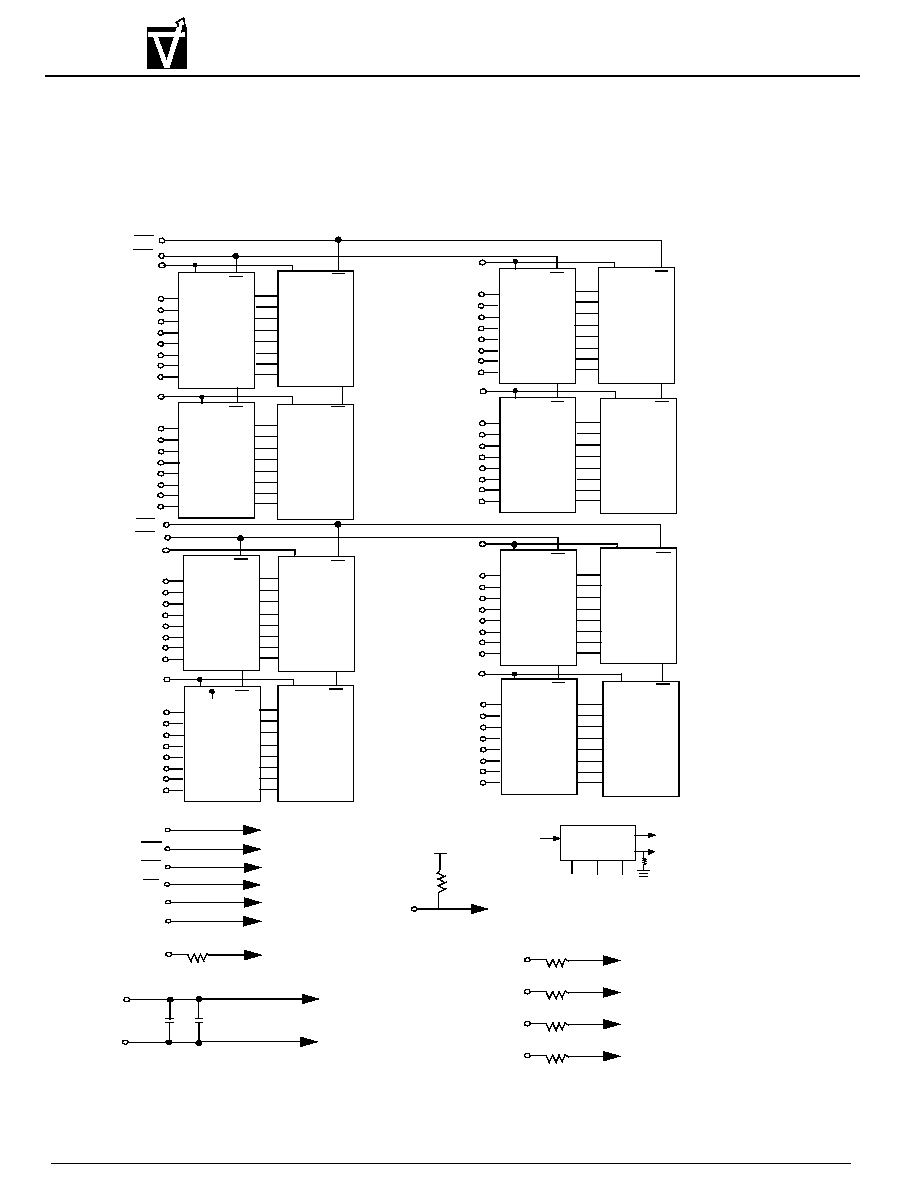
Functional Block Diagram (8M x 64)
CS0
DQMB0
DQ0
DQ1
DQ2
DQ4
DQ5
DQ6
DQ7
DQM
CS
UO
DQMB4
DQ32
DQ33
DQ34
DQ36
DQ37
DQ38
DQ39
DQM
CS
U4
DQ3
DQ35
DQ0
DQ1
DQ2
DQ4
DQ5
DQ6
DQ7
DQ3
DQ0
DQ1
DQ2
DQ4
DQ5
DQ6
DQ7
DQ3
DQMB1
DQ8
DQ9
DQ10
DQ12
DQ13
DQ14
DQ15
DQM
CS
U1
DQMB5
DQ40
DQ41
DQ42
DQ44
DQ45
DQ46
DQ47
DQM
CS
U5
DQ11
DQ43
DQ0
DQ1
DQ2
DQ4
DQ5
DQ6
DQ7
DQ3
DQ0
DQ1
DQ2
DQ4
DQ5
DQ6
DQ7
DQ3
CS2
DQMB2
DQ16
DQ17
DQ18
DQ20
DQ21
DQ22
DQ23
DQM
CS
U2
DQ19
DQ0
DQ1
DQ2
DQ4
DQ5
DQ6
DQ7
DQ3
DQMB3
DQ24
DQ25
DQ26
DQ28
DQ29
DQ30
DQ32
DQM
CS
U3
DQ27
DQ0
DQ1
DQ2
DQ4
DQ5
DQ6
DQ7
DQ3
DQMB6
DQ48
DQ49
DQ50
DQ52
DQ53
DQ54
DQ55
DQM
CS
U6
DQ51
DQ0
DQ1
DQ2
DQ4
DQ5
DQ6
DQ7
DQ3
DQMB7
DQ56
DQ57
DQ58
DQ60
DQ61
DQ62
DQ63
DQM
CS
U7
DQ59
DQ0
DQ1
DQ2
DQ4
DQ5
DQ6
DQ7
DQ3
RAS
CAS
WE
CKE0
A0 ~ A11
SDRAM U0 ~ U7
SDRAM U0 ~ U7
SDRAM U0 ~ U7
SDRAM U0 ~ U7
SDRAM U0 ~ U7
DQn
10
Every DQpin of SDRAM
V
DD
V
SS
To all SDRAMs
A0
A1
A2
SCL
Serial PD
SA0
SA1
SA2
SDA
WP
47K
0.1
F
µ
0.1
F
µ
SDRAM U0 ~ U7
BA0 & BA1
CLK0
10
CLK2
10
U0/U1/U4/U5
U2/U3/U6/U7
Document:1G5-0185
Rev.1
Page 4
VIS
VS864648041D,VS1664648041D
8M,16MX64-Bit
SDRAM Module
A0
A1
A2
SCL
Serial PD
SA0
SA1
SA2
SDA
WP
CS0
DQMB0
DQ0
DQ1
DQ2
DQ4
DQ5
DQ6
DQ7
DQM
CS
UO
DQMB4
DQ32
DQ33
DQ34
DQ36
DQ37
DQ38
DQ39
DQM
CS
U4
DQ3
DQ35
DQ0
DQ1
DQ2
DQ4
DQ5
DQ6
DQ7
DQ3
DQ0
DQ1
DQ2
DQ4
DQ5
DQ6
DQ7
DQ3
DQMB1
DQ8
DQ9
DQ10
DQ12
DQ13
DQ14
DQ15
DQM
CS
U1
DQMB5
DQ40
DQ41
DQ42
DQ44
DQ45
DQ46
DQ47
DQM
CS
U5
DQ11
DQ43
DQ0
DQ1
DQ2
DQ4
DQ5
DQ6
DQ7
DQ3
DQ0
DQ1
DQ2
DQ4
DQ5
DQ6
DQ7
DQ3
CS2
DQMB2
DQ16
DQ17
DQ18
DQ20
DQ21
DQ22
DQ23
DQM
CS
U2
DQ19
DQ0
DQ1
DQ2
DQ4
DQ5
DQ6
DQ7
DQ3
DQMB3
DQ24
DQ25
DQ26
DQ28
DQ29
DQ30
DQ31
DQM
CS
U3
DQ27
DQ0
DQ1
DQ2
DQ4
DQ5
DQ6
DQ7
DQ3
DQMB6
DQ48
DQ49
DQ50
DQ52
DQ53
DQ54
DQ55
DQ51
DQMB7
DQ56
DQ57
DQ58
DQ60
DQ61
DQ62
DQ63
DQM
CS
U7
DQ59
DQ0
DQ1
DQ2
DQ4
DQ5
DQ6
DQ7
DQ3
DQM
CS
U8
DQM
CS
U12
DQ0
DQ1
DQ2
DQ4
DQ5
DQ6
DQ7
DQ3
DQ0
DQ1
DQ2
DQ4
DQ5
DQ6
DQ7
DQ3
DQM
CS
U9
DQM
CS
U13
DQ0
DQ1
DQ2
DQ4
DQ5
DQ6
DQ7
DQ3
DQ0
DQ1
DQ2
DQ4
DQ5
DQ6
DQ7
DQ3
DQM
CS
U10
DQ0
DQ1
DQ2
DQ4
DQ5
DQ6
DQ7
DQ3
DQM
CS
U11
DQ0
DQ1
DQ2
DQ4
DQ5
DQ6
DQ7
DQ3
DQM
CS
U14
DQ0
DQ1
DQ2
DQ4
DQ5
DQ6
DQ7
DQ3
DQM
CS
U15
DQ0
DQ1
DQ2
DQ4
DQ5
DQ6
DQ7
DQ3
CS3
RAS
CAS
WE
CKE0
A0 ~ A11
SDRAM U0 ~ U15
SDRAM U0 ~ U15
SDRAM U0 ~ U15
SDRAM U0 ~ U15
SDRAM U0 ~ U15
DQn
10
Every DQpin of SDRAM
V
DD
V
SS
To all SDRAMs
10K
CKE1
V
CC
SDRAM U8 ~ U15
47K
Functional Block Diagram (16M x 64)
CS1
0.1
F
µ
0.1
F
µ
SDRAM U0 ~ U15
BA0 & BA1
DQM
CS
U6
DQ0
DQ1
DQ2
DQ4
DQ5
DQ6
DQ7
DQ3
CLK0
10
CLK1
10
CLK2
10
CLK3
10
U0/U1/U4/U5
U8/U9/U12/U13
U2/U3/U6/U7
U10/U11/U14/U15
Document:1G5-0185
Rev.1
Page 5
VIS
VS864648041D,VS1664648041D
8M,16MX64-Bit
SDRAM Module
Command Truth Table
FUNCTION
Symbol
CKE
CS
RAS
CAS
WE
BA
A10
A11
A9 - A0
n - 1
n
Device deselect
DESL
H
X
H
X
X
X
X
X
X
No operation
NOP
H
X
L
H
H
H
X
X
X
Mode register set
MRS
H
X
L
L
L
L
L
L
V
Bank activate
ACT
H
X
L
L
H
H
V
V
V
Read
READ
H
X
L
H
L
H
V
L
V
Read with auto pre-
charge
READA
H
X
L
H
L
H
V
H
V
Write
WRIT
H
X
L
H
L
L
V
L
V
Write with auto pre-
charge
WRITA
H
X
L
H
L
L
V
H
V
Precharge select
bank
PRE
H
X
L
L
H
L
V
L
X
Precharge all banks
PALL
H
X
L
L
H
L
X
H
X
Burst stop
BST
H
X
L
H
H
L
X
X
X
CBR (Auto) refresh
REF
H
H
L
L
L
H
X
X
X
Self refresh
SELF
H
L
L
L
L
H
X
X
X