1
White Electronic Designs Corporation ∑ (602) 437-1520 ∑ www.wedc.com
White Electronic Designs
EDI2GG464128V
October 2004
Rev. 1
4MB SYNCHRONOUS CARD EDGE DIMM
FEATURES
4x128Kx64
Synchronous
Access
Speed(s):
T
KHQV
= 9.5, 10, 11, 12, 15ns
Flow-Through
Architecture
Clock Controlled Registered Bank Enables (E1#,
E2#, E3#, E4#)
Clock Controlled Registered Address
Clock Controlled Registered Global Write (GW#)
Aysnchronous Output Enable (G#)
Internally self-timed Write
Gold Lead Finish
3.3V +10%, -5% Operation
Access Speed(s): t
KHQV
= 9.5, 10, 11, 12, 15ns
Common
Data
I/O
High Capacitance (30pf) drive, at rated Access
Speed
Single total array Clock
Multiple
Vcc
and
GND
DESCRIPTION
The EDI2KG64128VxxD is a Synchronous SRAM,
60 position Card Edge DIMM (120 contacts) Module,
or ga nized as 4x128Kx64. The Module con tains eight
(8) Syn chro nous Burst Ram Devices, packaged in the
in dus try standard JEDEC 14mmx20mm TQFP placed on
a Mul ti lay er FR4 Sub strate. The module architecture is
defi ned as a Synchronous Only, Flow-Through, Early Write
Device. This module provides High Performance, Ultra
Fast access times at a cost per bit benefi t over BiCMOS
Asynchronous SRAM based devices. As well as improved
cost per bit, the use of Synchronous or Synchronous Burst
devices or modules can ease the memory subsystem
design by reducing or easing the memory controller
requirement.
Synchronous operations are in relation to an externally
supplied clock, Registered Address, Registered Global
Write, Registered Enables as well as an Asynchronous
Output enable. All read and write operations to this module
are performed on Quad Words (64 bit op er a tions).
Write cycles are internally self timed and are initiated by
a rising clock edge. This feature relieves the designer the
task of developing external write pulse width cir cuit ry.
*This product is subject to change without notice.
PIN NAMES
DQ0-DQ63
Input/Output Bus
A015
Address Bus
E1#, E2#,
E3#, E4#
Synchronous Bank Enables
CK
Array Clock
GW#
Synchronous Global Write Enable
G#
Asynchronous Output Enable
Vcc
3.3V Power Supply
Vss
Ground
NC
No Connect
2
White Electronic Designs Corporation ∑ (602) 437-1520 ∑ www.wedc.com
White Electronic Designs
EDI2GG464128V
October 2004
Rev. 1
PIN CONFIGURATION
V
SS
A
0
A
1
A
2
A
3
V
CC
A
4
A
5
A
6
A
7
V
SS
A
8
V
SS
CK
V
SS
E
4
#
V
CC
E
3
#
G#
V
SS
DQ
0
DQ
1
DQ
2
DQ
3
V
CC
DQ
8
V
SS
A
16
A
15
A
14
A
13
V
CC
A
12
A
11
A
10
A
9
V
SS
RFU
V
SS
NC
V
SS
E
2
#
V
CC
E
1
#
GW#
V
SS
DQ
7
DQ
6
DQ
5
DQ
4
V
CC
DQ
15
DQ
9
DQ
10
DQ
11
V
SS
DQ
16
DQ
17
DQ
18
DQ
19
V
CC
DQ
24
DQ
25
DQ
26
DQ
27
V
SS
DQ
32
DQ
33
DQ
34
DQ
35
V
CC
DQ
40
DQ
41
DQ
42
DQ
43
V
SS
DQ
48
DQ
49
DQ
50
DQ
51
V
CC
DQ
56
DQ
57
DQ
58
DQ
59
V
SS
DQ
14
DQ
13
DQ
12
V
SS
DQ
23
DQ
22
DQ
21
DQ
20
V
CC
DQ
31
DQ
30
DQ
29
DQ
28
V
SS
DQ
39
DQ
38
DQ
34
DQ
37
V
CC
DQ
47
DQ
46
DQ
45
DQ
44
V
SS
DQ
55
DQ
54
DQ
53
DQ
52
V
CC
DQ
63
DQ
62
DQ
61
DQ
60
V
SS
11
13
15
17
19
21
23
25
27
28
26
24
22
20
18
16
14
12
10
29
31
33
35
37
39
41
43
45
47
49
51
52
50
48
46
44
42
40
38
36
34
30
32
53
55
57
59
61
63
65
67
69
71
73
54
56
58
60
62
64
66
68
70
72
74
75
77
79
81
83
85
87
89
91
93
76
78
80
82
84
86
88
90
92
94
96
98
100
102
104
106
108
110
112
114
116
95
97
99
101
103
105
107
109
111
113
115
117
119
118
120
3
5
7
9
1
8
6
4
2
3
White Electronic Designs Corporation ∑ (602) 437-1520 ∑ www.wedc.com
White Electronic Designs
EDI2GG464128V
October 2004
Rev. 1
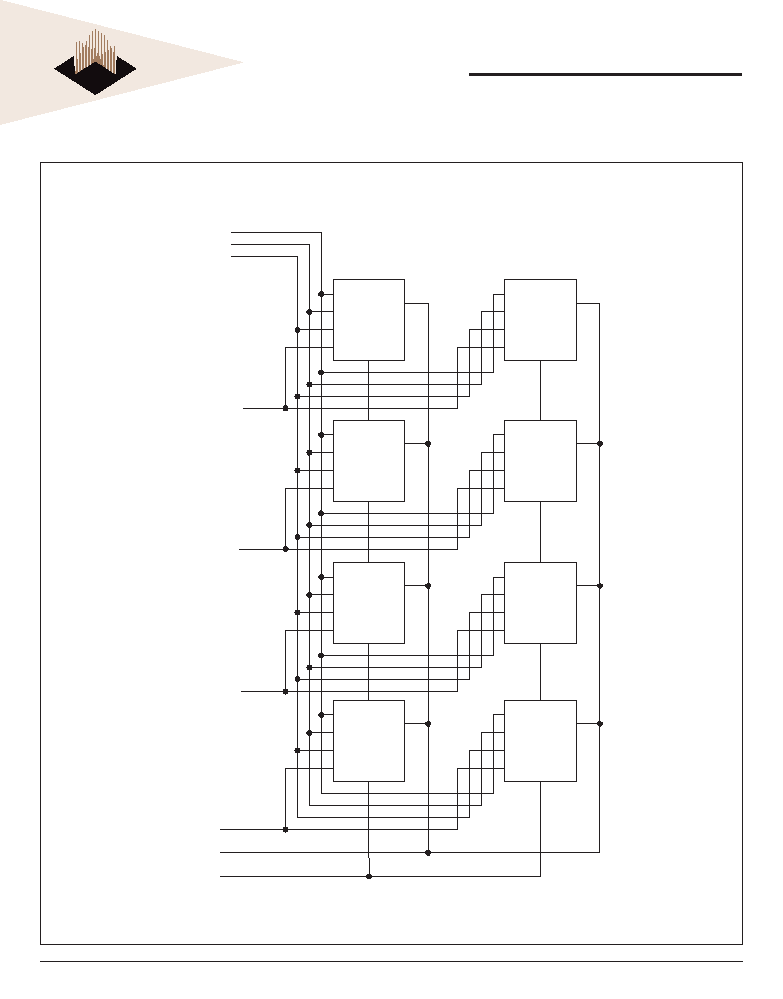
FUNCTIONAL BLOCK DIAGRAM
G#
GW#
E
1
#
E
3#
GW
G#
E#
DQ
GW
G#
E#
DQ
E
2
#
E
4#
CLK
CLK
CLK
A
0-16
GW#
G#
E#
DQ
CLK
128Kx32
GW#
G#
E#
DQ
CLK
128Kx32
GW#
G#
E#
DQ
CLK
128Kx32
GW#
G#
E#
DQ
CLK
128Kx32
GW#
G#
E#
DQ
CLK
128Kx32
GW#
G#
E#
DQ
CLK
128Kx32
128Kx32
128Kx32
DQ
0-63
4
White Electronic Designs Corporation ∑ (602) 437-1520 ∑ www.wedc.com
White Electronic Designs
EDI2GG464128V
October 2004
Rev. 1
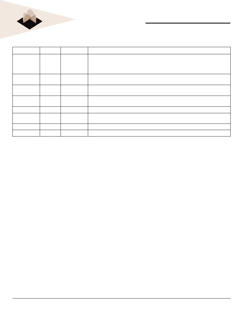
PIN DESCRIPTIONS
DIMM Pins
Symbol
Type
Description
3, 5, 7, 9, 13,
15, 17, 19, 20,
23, 18, 16, 14,
10, 8, 6
A0-A15
Input
Synchronous
Addresses: These inputs are registered and must meet the setup and hold times around the rising edge of
CK. The burst counter generates internal addresses associated with A
0
and A
1
, during burst and wait cycle.
38
GW#
Input
Synchronous
Global Write: This active LOW input allows a full 72-bit WRITE to occur independent of the BWE# and BWx#
lines and must meet the setup and hold times around the rising edge of CK.
27
CK
Input
Synchronous
Clock: This signal registers the addresses, data, chip enables, write control and burst control inputs on its
rising edge. All synchronous inputs must meet setup and hold times around the clock's rising edge.
36, 32,
35, 31
E1#, E2#
E3#, E4#
Input
Synchronous
Bank Enables: These active LOW inputs are used to enable each individual Synchronous bank and to gate
ADSP#.
37
G#
Input
Output Enable: This active LOW asynchronous input enables the data output drivers.
Various
DQ0-63
Input/Output
Data Inputs/Outputs: First byte is DQ
0-7
, second byte is DQ
8-15
, third byte is DQ
16-23
, fourth byte is DQ
24-31
,
fi fth byte is DQ
32-39
, sixth byte is DQ
40-47
, seventh byte is DQ
48-55
and the eight byte is DQ
56-64
.
Various
Vcc
Supply
Core power supply: +3.3V -5%/+10%
Various
Vss
Ground
Ground
5
White Electronic Designs Corporation ∑ (602) 437-1520 ∑ www.wedc.com
White Electronic Designs
EDI2GG464128V
October 2004
Rev. 1
ABSOLUTE MAXIMUM RATINGS*
Voltage on Vcc Relative to Vss
-0.5V to +4.6V
V
IN
-0.5V to Vcc +0.5V
Storage Temperature
-55∞C to +125∞C
Operating Temperature (Commercial)
0∞C to +70∞C
Operating Temperature (Industrial)
-40∞C to +85∞C
Short Circuit Output Current
20 mA
* Stress greater than those listed under "Absolute Maximum Ratings" may cause
permanent damage to the device. This is a stress rating only and functional
operation of the device at these or any other conditions greater than those indicated
in operational sections of this specifi cations is not implied. Exposure to absolute
maximum rating conditions for extended periods may affect reliability.
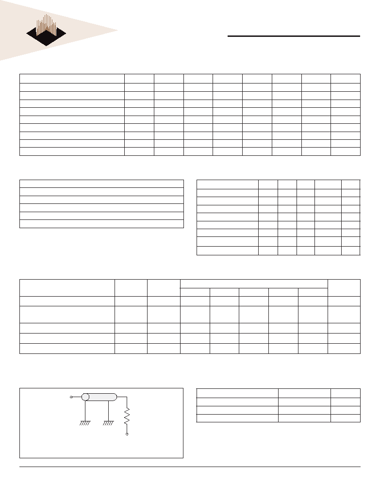
AC TEST LOAD
SYNCHRONOUS ONLY ≠ TRUTH TABLE
Operation
E1#
E2#
E3#
E4#
GW#
G#
CK
DQ
Synchronous Write-Bank 1
L
H
H
H
L
H
High-Z
Synchronous Read-Bank 1
L
H
H
H
H
L
Synchronous Write-Bank 2
H
L
H
H
L
H
High-Z
Synchronous Read-Bank 2
H
L
H
H
H
L
Synchronous Write-Bank 3
H
H
L
H
L
H
High-Z
Synchronous Read-Bank 3
H
H
L
H
H
L
Synchronous Write-Bank 4
H
H
H
L
L
H
High-Z
Synchronous Read-Bank 4
H
H
H
L
H
L
Snooze Mode
X
X
X
X
X
X
X
High-Z
AC TEST CONDITIONS
Parameter
I/O
Unit
Input Pulse Levels
Vss to 3.0V
V
Input and Output Timing Ref.
1.25
V
Output Test Equivalencies
See fi gure at left
V
RECOMMENDED DC OPERATING CON DI TIONS
Parameter
Sym
Min
Typ
Max
Units
Supply Voltage
V
CC
3.14
3.3
3.6
V
Supply Voltage
V
SS
0.0
0.0
0.0
V
Input High
V
IH
2.2
3.0
V
CC
+ 0.3
V
Input Low
V
IL
-0.3 0.0
0.8
V
Input Leakage
I
LI
-2
1
2
µA
Output Leakage
I
LO
-2
1
2
µA
Output High I
OH
= -4ma
V
OH
2.4
-
-
V
Output Low I
OL
= 8ma
V
OL
-
-
0.4
V
DC ELECTRICAL CHARACTERISTICS ≠ READ CYCLE
Description
Symbol
Typ
Max
Units
9.5
10
11
12
15
Power Supply Current
Icc1
1.55
2.8
2.2
2.2
2.7
2.0
A
Power Supply Current
Device Selected, No Operation
Icc
.75
1.8
1.5
1.3
1.3
1.0
A
Snooze Mode
IccZZ
200
300
300
300
300
300
mA
CMOS Standby
Icc3
400
500
500
500
500
500
mA
Clock Running-Deselect
IccK
600
900
900
900
900
900
mA
*TBD
50
Vt = 1.25V
DQ
Z0 = 50W
Z0 = 50
Figure 1 ≠ Output Load Equivalent