
EDI7F4342MV
1
White Electronic Designs Corporation ∑ (602) 437-1520 ∑ www.wedc.com
White Electronic Designs
Sept. 2002 Rev. 1A
White Electronic Designs Corp. reserves the right to change products or specifications without notice.
n
4x2Mx32
n
Based on Intel's E28F016S3 Flash Device
n
Fast Read Access Time - 120ns
n
Flexible Smart Voltage
n
2.7-3.6V Program Erase
n
2.7-3.6V Read Operation
n
12Vpp Fast Production Programming
n
Low Power Dissipation
n
30mA per Device Active Current
n
20µA per Device CMOS Standby Current
n
Typical Endurance >100,000 Cycles
n
Single 3.0V -10%, +20% Supply
n
CMOS and TTL Compatible Inputs and Outputs
n
Commercial and Industrial Temperature Range
n
Package
n
80 Pin SIMM (JEDEC)
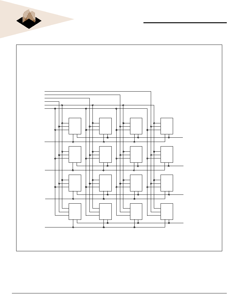
The EDI7F4342MV is organized as four banks of 2Mx32.
The module is based on Intel's E28F016S3 - 2Mx8 Flash
device in TSOP packages which are mounted on an FR4
substrate.
The module offers access times between 120 and 150ns
allowing for operation of high-speed microprocessors
without wait states.
*This product is subject to change without notice.
FEATURES
DESCRIPTION
4x2Mx32 FLASH MODULE
EDI7F4342MV
2
White Electronic Designs Corporation ∑ (602) 437-1520 ∑ www.wedc.com
White Electronic Designs
Sept. 2002 Rev. 1A
White Electronic Designs Corp. reserves the right to change products or specifications without notice.
EDI7F4342MV-BNC: 4x2Mx32 80 PIN SIMM
FIG. 1
BLOCK DIAGRAM
EDI7F4342MV
3
White Electronic Designs Corporation ∑ (602) 437-1520 ∑ www.wedc.com
White Electronic Designs
Sept. 2002 Rev. 1A
White Electronic Designs Corp. reserves the right to change products or specifications without notice.
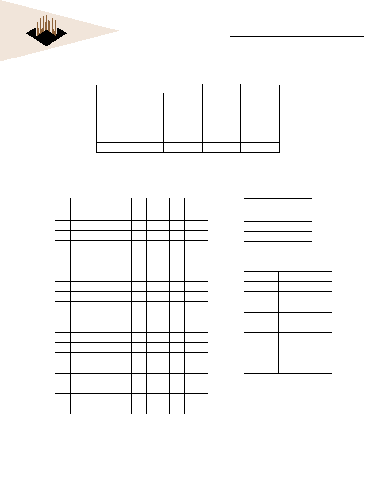
PIN CONFIGURATIONS
A0-A20
Address Input
E0#,-E3#
Chip Enable
W0#-W3#
Write Enable
G#
Output Enable
DQ0-DQ31
Data Input/Output
P
D
Presence Detect
V
CC
Power 3V -10% +20%
V
SS
Ground
NC
No Connect
V
PP
Program Power
CAPACITANCE
(f=1.0MHz, V
IN
= V
CC
or V
SS
)
Presence Detect Pin Out
Pin
4X2Meg
PD1
V
SS
PD2
V
SS
PD3
V
SS
PD4
V
SS
Pin
Name
Pin
Name
Pin
Name
Pin
Name
1
V
SS
21
E3#
41
A11
61
DQ9
2
V
CC
22
E2#
42
A10
62
DQ8
3
V
PP
23
E1#
43
A9
63
DQ7
4
G#
24
E0#
44
A8
64
DQ6
5
W0#
25
V
SS
45
A7
65
DQ5
6
W1#
26
DQ29
46
A6
66
DQ4
7
NC
27
DQ30
47
A5
67
DQ3
8
DQ16
28
DQ31
48
A4
68
DQ2
9
DQ17
29
W2#
49
A3
69
DQ1
10
DQ18
30
NC
50
A2
70
DQ0
11
DQ19
31
NC
51
A1
71
V
PP
12
DQ20
32
NC
52
AO
72
V
CC
13
DQ21
33
A19
53
W3#
73
PD1
14
DQ22
34
A18
54
V
SS
74
PD2
15
DQ23
35
A17
55
DQ15
75
PD3
16
DQ24
36
A16
56
DQ14
76
PD4
17
DQ25
37
A15
57
DQ13
77
PD5
18
DQ26
38
A14
58
DQ12
78
PD6
19
DQ27
39
A13
59
DQ11
79
PD7
20
DQ28
40
A12
60
DQ10
80
V
SS
4x2Meg
Parameter
Sym
Max
Unit
Address Lines
CA
140
pF
Data lines
CDQ
60
pF
Chip & Write
Enable Lines
CC
60
pF
Output Enable lines
CG
140
pF

EDI7F4342MV
4
White Electronic Designs Corporation ∑ (602) 437-1520 ∑ www.wedc.com
White Electronic Designs
Sept. 2002 Rev. 1A
White Electronic Designs Corp. reserves the right to change products or specifications without notice.
ORDERING INFORMATION
PACKAGE NO. 394: 80 PIN SIMM (JEDEC)
Part Number
Speed
(ns)
Package
EDI7F4342MV120BNC
120
394
EDI7F4342MV150BNC
150
394
ALL DIMENSIONS ARE IN INCHES