
1
White Electronic Designs Corporation ∑ (602) 437-1520 ∑ www.wedc.com
White Electronic Designs
EDI7F292MC
EDI7F492MC
January 2006
Rev. 1
PRELIMINARY*
ARCHITECHTURE
FEATURES
5.0 Volt ± 10% fi r read and write operations
∑ Minimizes system level power requirements
Compatible with JEDEC-standards
∑ Pinout and software compatible with single-power
supply Flash
∑ Superior inadvertent write protection
80 SIMM (JEDEC)
Minimum 100,000 write/erase cycles guaranteed
High
performance
∑ 70 ns maximum access time
Sector erase architecture
∑ Uniform sectors of 64 Kbytes each
∑ Any combination of sectors can be erased. Also
supports full chip erase
Group sector protection
∑ Hardware method that disables any combination
of sector groups from write or erase operations
(a sector group consists of 4 adjacent sectors of
64Kbytes each)
Embedded
Erase
Algorithms
∑ Automatically pre-programs and erases the chip
or any sector
Embedded
Program
Algorithms
∑ Automatically programs and verifi es data at
specifi ed address
Data# Polling and Toggle Bit feature for detection
of program or erase cycle completion
Ready/Busy# output (RY/BY#)
∑ Hardware method for detection of program or
erase cycle completion
Erase
Suspend/Resume
∑ Supports reading or programming data to a
sector not being erased
Low power consumption (EDI7292MC)
∑ 50 mA typical active read current
∑ 60 mA typical program/erase current
Low power consumption (EDI7492MC)
4MB/8MB (2x2Mx8 / 4x2Mx8) Flash Module 5.0V, Boot-Only
Sector Erase Flash Memory
∑ 100 mA typical active read current
∑ 120 mA typical program/erase current
Enhanced power management for standby mode
∑ <1 µA typical standby current
∑ Standard access time from standby mode
Hardware RESET# pin
∑ Resets internal state machine to the read mode
* This product is under development, is not qualifi ed or characterized and is subject to
change without notice.
DESCRIPTION
The EDI7F292/492MC is a 32/64 Mbit, 5.0 Volt-only
Flash memory organized as 2 Megabytes of 8 bits each.
The 2Mbytes of data is divided into 32 sectors of 64
Kbytes for fl exible erase capability. The 8 bits of data
appear on DQ0≠DQ7. The EDI7F292/492MC is offered
in 80 Pin SIMM packages. This device is designed to be
programmed in-system with the standard system 5.0 Volt
V
CC
supply. 12.0 Volt V
PP
is not required for program or
erase operations. The device can also be reprogrammed
in standard EPROM programmers.
The standard EDI7F292/492MC offers access times of 100
ns, and 120 ns, allowing high-speed microprocessors to
operate without wait states. To eliminate bus contention,
the device has separate chip enable 4 CS#, write enable
WE#, and output enable OE# controls.
The EDI7F292/492MC is entirely command set compatible
with the JEDEC single-power supply Flash standard.
Commands are written to the command register using
standard microprocessor write timings. Register contents
serve as input to an internal state-machine that controls
the erase and programming circuitry. Write cycles also
internally latch addresses and data needed for the
programming and erase operations. Reading data out
of the device is similar to reading from 12.0 Volt Flash or
EPROM devices.
The EDI7F292/492MC is programmed by executing
the program command sequence. This will invoke the
Embedded Program Algorithm which is an internal
algorithm that automatically times the program pulse widths
and verifi es proper cell margin. Erase is accomplished by
2
White Electronic Designs Corporation ∑ (602) 437-1520 ∑ www.wedc.com
White Electronic Designs
EDI7F292MC
EDI7F492MC
January 2006
Rev. 1
PRELIMINARY
executing the erase command sequence. This will invoke
the Embedded Erase Algorithm which is an internal
algorithm that automatically preprograms the array if it
is not already programmed before executing the erase
operation. During erase, the device automatically times the
erase pulse widths and verifi es proper cell margin.
This device also features a sector erase architecture.
This allows for sectors of memory to be erased and
reprogrammed without affecting the data contents of
other sectors. A sector is typically erased and verifi ed
within one second. The EDI7F292/492MC is erased when
shipped .
The EDI7F292/492MC device also features hardware
sector group protection. This feature will disable both
program and erase operations in any combination of
eight sector groups of memory. A sector group consists
of four adjacent sectors grouped in the following pattern:
sectors 0≠3, 4≠7, 8≠11, 12≠15, 16≠19, 20≠23, 24≠27,
and 28≠31.
WEDC has implemented an Erase Suspend feature that
enables the user to put erase on hold for any period of
time to read data from, or program data to, a sector that
was not being erased. Thus, true background erase can
be achieved.
The device features single 5.0 Volt power supply operation
for both read and write functions. Internally generated and
regulated voltages are provided for the program and erase
operations. A low V
CC
detector automatically inhibits write
operations during power transitions. The end of program
or erase is detected by the RY/BY# pin, Data# polling
of DQ7, or by the Toggle Bit I (DQ6). Once the end of a
program or erase cycle has been completed, the device
automatically resets to the read mode.
The EDI7F292/492MC also has a hardware RESET# pin.
When this pin is driven low, execution of any Embedded
Program Algorithm or Embedded Erase Algorithm will be
terminated. The internal state machine will then be reset
into the read mode. The RESET# pin may be tied to the
system reset circuitry. Therefore, if a system reset occurs
during the Embedded Program Algorithm or Embedded
Erase Algorithm, the device will be automatically
reset to the read mode. This will enable the system's
microprocessor to read the boot-up fi rmware from the
Flash memory.
The EDI7F292/492MC memory electrically erases all
bits within a sector simultaneously via Fowler-Nordheim
tunneling. The bytes are programmed one byte at a time
using the EPROM programming mechanism of hot electron
injection.
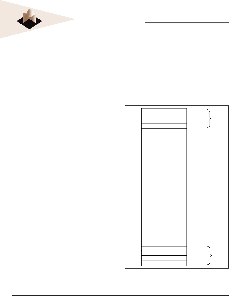
FLEXIBLE SECTOR-ERASE
Thirty two 64 Kbyte sectors
Eight sector groups each of which consists of 4
adjacent sectors in the following pattern: sectors 0-
3, 4-7, 8-11, 12-15, 16-19, 20-23, 24-27, and 28-31.
Individual-sector or multiple-sector erase capability
Sector group protection is user-defi nable
SA31
SA30
SA29
SA28
SA3
SA2
SA1
SA0
1FFFFFh
1EFFFFh
1DFFFFh
1CFFFFh
1BFFFFh
1AFFFFh
19FFFFh
18FFFFh
17FFFFh
16FFFFh
15FFFFh
14FFFFh
13FFFFh
12FFFFh
11FFFFh
10FFFFh
1FFFFFh
1EFFFFh
1DFFFFh
1CFFFFh
1BFFFFh
1AFFFFh
09FFFFh
08FFFFh
07FFFFh
06FFFFh
05FFFFh
04FFFFh
03FFFFh
02FFFFh
01FFFFh
00FFFFh
000000h
Sector
Group
7
Sector
Group
0
64 Kbyte
64 Kbyte
64 Kbyte
64 Kbyte
64 Kbyte
64 Kbyte
64 Kbyte
64 Kbyte
32 Sectors Total

3
White Electronic Designs Corporation ∑ (602) 437-1520 ∑ www.wedc.com
White Electronic Designs
EDI7F292MC
EDI7F492MC
January 2006
Rev. 1
PRELIMINARY
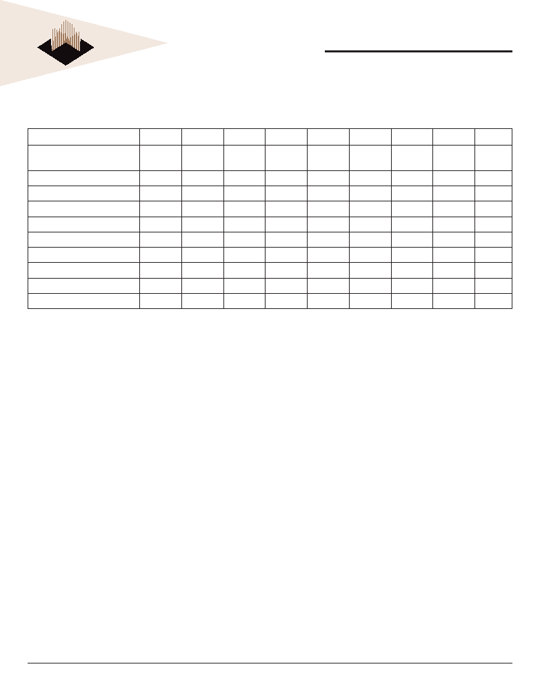
PRODUCT SELECTOR GUIDE
Family Part No.
Symbol
Symbol
Ordering Park No.
V
CC
= 5.0 Volt ± 5%
V
CC
= 5.0 Volt ± 10%
-100
-120
Max Access Time (ns)
100
120
CS# Access (ns)
100
120
OE# Access (ns)
50
Block Diagrams
EDI7F292MC-BNC: 2x2Mx8 80 PIN SIMM
FIG. 1
EDI7F492MC-BNC: 4x2Mx8 80 PIN SIMM
A0-A20
OE#
RESET#
WE#
CS
0
#
CS
1
#
2Mx8
2Mx8
DQ0-DQ7
A0-A20
OE#
RESET#
WE#
CS
0
#
CS
1
#
CS
2
#
CS
3
#
2Mx8
2Mx8
2Mx8
2Mx8
DQ0-D
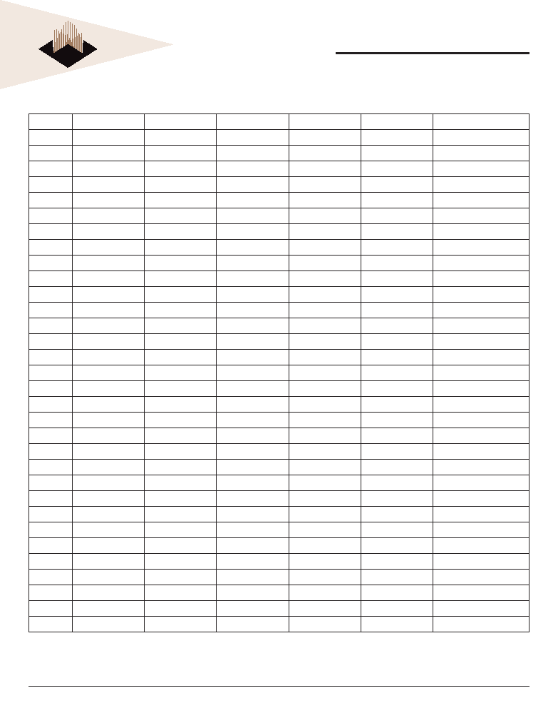
PIN CONFIGURATIONS
Pin
#
Pin
Name
Pin
#
Pin
Name
Pin
#
Pin
Name
Pin
#
Pin
Name
1
V
SS
21
CS#
41
A11
61
NC
2
V
CC
22
CS#
42
A10
62
NC
3
NC
23
CS#
43
A9
63
DQ7
4
OE#
24
CS#
44
A8
64
DQ6
5
WE#
25
V
SS
45
A7
65
DQ5
6
NC
26
NC
461
A6
66
DQ4
7
RESET#
27
NC
47
A5
67
DQ3
8
NC
28
NC
48
A4
68
DQ2
9
NC
29
NC
49
A3
69
DQ1
10
NC
30
NC
50
A2
70
DQ0
11
NC
31
NC
51
A1
71
NC
12
NC
32
A20
52
A0
72
V
CC
13
NC
33
A19
53
NC
73
PD1/NC
14
NC
34
A18
54
V
SS
74
PD2/NC
15
NC
35
A17
55
NC
75
PD3/NC
16
NC
36
A16
56
NC
76
PD4/NC
17
NC
37
A15
57
NC
77
PD5/NC
18
NC
38
A14
58
NC
78
PD6/NC
19
NC
39
A13
59
NC
79
PD7/NC
20
NC
40
A12
60
NC
80
V
SS
Note: Pins 21 and 22 are not connected for EDI7F292MC.
A0-A20
Address input
CS
0
- CS
3
#
Chip Enable
WE#
Write Enable
OE#
Output Enable
DQ0-DQ7
Data Input/Output
PD1-PD7/NC*
Presence Detect
RP
Reset Pin
V
CC
Power 5V±10%
V
SS
Ground
NC
No Connect
*Contact factors if PD pin's are needed.
4
White Electronic Designs Corporation ∑ (602) 437-1520 ∑ www.wedc.com
White Electronic Designs
EDI7F292MC
EDI7F492MC
January 2006
Rev. 1
PRELIMINARY
TABLE 1. EDI7F292/492MC USER BUS OPERATIONS
Module Organization
CS#
OE#
WE#
A0
A1
A6
A9
DQ0-DQ7
RESET#
Autoselect, WEDC Manuf. Code
(1)
L
L
H
L
L
L
V
ID
Code
H
Autoselect Device Code (1)
L
L
H
H
L
L
V
ID
Code
H
Read
L
L
X
A0
A1
A6
A9
D
OUT
H
Standby
H
X
X
X
X
X
X
HIGH Z
H
Output Disable
L
H
H
X
X
X
X
HIGH Z
H
Write
L
H
L
A0
A1
A6
A9
D
IN
H
Enable Sector Group Protect (2)
L
V
ID
L
X
X
X
V
ID
X
H
Verify Sector Group Protect (2)
L
L
H
L
H
L
V
ID
Code
H
Temporary Sector Group Unprotect
X
X
X
X
X
X
X
X
VID
Hardware Reset/Standby
X
X
X
X
X
X
X
HIGH Z
L
Legend:
L = logic 0, H = logic 1, X = Don't Care. See DC Characteristics for voltage levels.
Notes:
1.
Manufacturer and device codes may also be accessed via a command register write sequence. Refer to Table 5.
2.
Refer to the section on Sector Group Protection.
READ MODE
The EDI7F292/492MC has two control functions which
must be satisfi ed in order to obtain data at the outputs.
CS# is the power control and should be used for device
selection . OE# is the output control and should be used to
gate data to the output pins if the device is selected.
Address access time (t
ACC
) is equal to the delay from stable
addresses to valid output data. The chip enable access
time (t
CS
) is the delay from stable addresses and stable
CS# to valid data at the output pins. The output enable
access time is the delay from the falling edge of OE# to
valid data at the output pins (assuming the addresses have
been stable for at lease t
ACC
-t
OE
time).
STANDBY MODE
There are two ways to implement the standby mode on
the EDI7F292/492MC device, one using both the CS# and
RESET# pins; the other via the RESET# pin only.
When using both pins, a CMOS standby mode is achieved
with CS# and RESET# inputs both held at V
CC
± 0.3V.
Under this condition the current is typically reduced to
less than 1 µA. A TTL standby mode is achieved with CS#
and RESET# pins held at V
IH
. Under this condition the
current is typically reduced to 200 µA. The device can be
read with standard access time (t
CS
) from either of these
stanby modes.
When using the RESET# pin only, a CMOS standby mode
is achieved with RESET# input held at VSS ± 0.3V (CS#
= don't care). Under this condition the current is typically
reduced to less than 1 µA. A TTL standby mode is achieved
with RESET# pin held at V
IL
(CS# = don't care). Under
this condition the current is typically reduced to less than
200 µA. One the RESET# pin is taken high, the device
requires 50 ns of wake up time before outputs are valid
for read access.
In the standby mode the outputs are in the high impedance
state, independent of the OE# input.
OUTPUT DISABLE
With the OE# input at a logic high level (V
IH
), output from
the device is disabled. This will cause the output pins to
be in a high impedance state.

5
White Electronic Designs Corporation ∑ (602) 437-1520 ∑ www.wedc.com
White Electronic Designs
EDI7F292MC
EDI7F492MC
January 2006
Rev. 1
PRELIMINARY
AUTOSELECT
The autoselect mode allows the reading of a binary code
from the device and will identify its manufacturer and
type. This mode is intended for use by programming
equipment for the purpose of automatically matching
the device to be programmed with its corresponding
programming algorithm. This mode is functional over the
entire temperature range of the device.
To activate this mode, the programming equipment must
force VID (11.5 V to 12.5 V) on address pin A9. Two
identifi er bytes may then be sequenced from the device
outputs by toggling address A0 from V
IL
to V
IH
All addresses
are don't cares except A0, A1, and A6 (seeTable 2).
The manufacturer and device codes may also be
read via the command register, for instances when
the EDI7F292/492MC is erased or programmed in a
system without access to high voltage on the A9 pin. The
command sequence is illustrated in Table 5 (see Autoselect
Command Sequence).
Byte 0 (A0 = V
IL
) ) represents the manufacturer's code
(WEDC = 01h) and byte 1 (A0 = V
IH
) the device identifi er
code for EDI7F292/492MC = ADh. These two bytes are
given in the table below. All identifi ers for manufacturer
and device will exhibit odd parity with DQ7 defi ned as the
parity bit. In order to read the proper device codes when
executing the Autoselect, A1 must be V
IL
(see Table 2).
The autoselect mode also facilitates the determination
of sector group protection in the system. By performing
a read operation at the address location XX02h with the
higher order address bits A18, A19, and A20 set to the
desired sector group address, the device will return 01h
for a protected sector group and 00h for a non-protected
sector group.
TABLE 2. EDI7F292/492MC SECTOR PROTECTION VERIFY AUTOSELECT CODES
Type
A18 to A20
A6
A1
A0
Code
(HEX)
DQ7
DQ6
DQ5
DQ4
DQ3
DQ2
DQ1
DQ0
Manufacture Code-WEDC
X
X
X
V
IL
V
IL
V
IL
01H
0
0
0
0
0
0
0
1
EDI7F292/492MC Devis
X
X
X
V
IL
V
IL
V
IH
ADH
1
0
1
0
1
1
0
1
Sector Group Protection
Sector Group
Address
V
IL
V
IH
V
IL
01H*
0
0
0
0
0
0
0
1
* Outputs 01H at protected sector addresses
6
White Electronic Designs Corporation ∑ (602) 437-1520 ∑ www.wedc.com
White Electronic Designs
EDI7F292MC
EDI7F492MC
January 2006
Rev. 1
PRELIMINARY
TABLE 3. SECTOR ADDRESS TABLE
A20
A19
A18
A17
A16
Address Range
SA0
0
0
0
0
0
000000h-00FFFFh
SA1
0
0
0
0
1
010000h-01FFFFh
SA2
0
0
0
1
0
020000h-02FFFFh
SA3
0
0
0
1
1
030000h-03FFFFh
SA4
0
0
1
0
0
040000h-04FFFFh
SA5
0
0
1
0
1
050000h-05FFFFh
SA6
0
0
1
1
0
060000h-06FFFFh
SA7
0
0
1
1
1
070000h-07FFFFh
SA8
0
1
0
0
0
080000h-08FFFFh
SA9
0
1
0
0
1
090000h-09FFFFh
SA10
0
1
0
1
0
0A10000h-0AFFFFh
SA11
0
1
0
1
1
0B0000h-0BFFFFh
SA12
0
1
1
0
0
0C0000h-0CFFFFh
SA13
0
1
1
0
1
0D0000h-0DFFFFh
SA14
0
1
1
1
0
0E0000h-0EFFFFh
SA15
0
1
1
1
1
0F0000h-0FFFFFh
SA16
1
0
0
0
0
100000h-10FFFFh
SA17
1
0
0
0
1
110000h-11FFFFh
SA18
1
0
0
1
0
120000h-12FFFFh
SA19
1
0
0
1
1
130000h-13FFFFh
SA20
1
0
1
0
0
140000h-14FFFFh
SA21
1
0
1
0
1
150000h-15FFFFh
SA22
1
0
1
1
0
160000h-16FFFFh
SA23
1
0
1
1
1
170000h-17FFFFh
SA24
1
0
0
0
0
180000h-18FFFFh
SA25
1
1
0
0
1
190000h-19FFFFh
SA26
1
1
0
1
0
1A0000h-1AFFFFh
SA27
1
1
0
1
1
1B0000h-1BFFFFh
SA28
1
1
1
0
0
1C0000h-1CFFFFh
SA29
1
1
1
0
1
1D0000h-1DFFFFh
SA30
1
1
1
1
0
1E0000h-1EFFFFh
SA31
1
1
1
1
1
1F0000h-1FFFFFh

7
White Electronic Designs Corporation ∑ (602) 437-1520 ∑ www.wedc.com
White Electronic Designs
EDI7F292MC
EDI7F492MC
January 2006
Rev. 1
PRELIMINARY
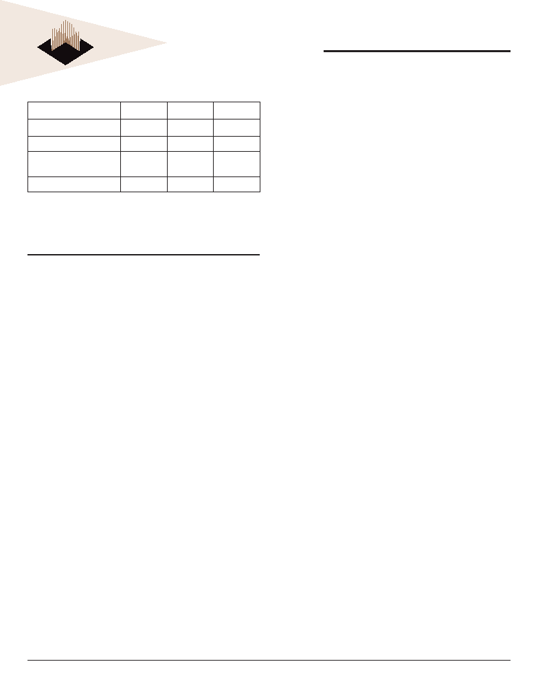
TABLE 4. SECTOR GROUP ADDRESS
A20
A19
A18
Sectors
SGA0
0
0
0
SA0-SA3
SGA1
0
0
1
SA4-SA7
SGA2
0
1
0
SA8-SA11
SGA3
0
1
1
SA12-SA15
SGA4
1
0
0
SA16-SA19
SGA5
1
0
1
SA20-SA23
SGA6
1
1
0
SA24-SA27
SGA7
1
1
1
SA28-SA31
WRITE
Device erasure and programming are accomplished via
the command register. The contents of the register serve
as inputs to the internal state machine. The state machine
outputs dictate the function of the device.
The command register itself does not occupy any
addressable memory location. The register is a latch
used to store the commands, along with the address and
data information needed to execute the command. The
command register is written to by bringing WE# to V
IL
, while
CS# is at V
IL
and OE# is at V
IH
. Addresses are latched on
the falling edge of WE# or CS#, whichever happens later;
while data is latched on the rising edge of WE# or CS#,
whichever happens fi rst. Standard microprocessor write
timings are used.
Refer to AC Write Characteristics and the Erase/
Programming Waveforms for specifi c timing parameters.
SECTOR GROUP PROTECTION
The EDI7F292/492MC features hardware sector group
protection. This feature will disable both program and
erase operations in any combination of eight sector groups
of memory. Each sector group consists of four adjacent
sectors grouped in the following pattern: sectors 0-3,
4-7, 8-11, 12-15, 16-19, 20-23, 24-27, and 28-31 (see
Table 4). The sector group protect feature is enabled
using programming equipment at the user's site. The
device is shipped with all sector groups unprotected. It is
possible to determine if a sector group is protected in the
system by writing an Autoselect command. Performing
a read operation at the address location XX02h, where
the higher order address bits A18, A19, and A20 is the
desired sector group address, will produce a logical "1"
at DQ0 for a protected sector group. See Table 2 for
Autoselect codes.
TEMPORARY SECTOR GROUP
UNPROTECT
This feature allows temporary unprotection of previously
protected sector groups of the EDI7F292/492MC device
in order to change data in-system. The Sector Group
Unprotect mode is activated by setting the RESET# pin to
high voltage (12V). During this mode, formerly protected
sector groups can be programmed or erased by selecting
the sector group addresses. Once the 12 V is taken away
from the RESET# pin, all the previously protected sector
groups will be protected again. Refer to Figures 15 and
16.
COMMAND DEFINITIONS
Device operations are selected by writing specifi c address
and data sequences into the command register. Writing
incorrect address and data values or writing them in
the improper sequence will reset the device to the
read mode. Table 5 defi nes the valid register command
sequences. Note that the Erase Suspend (B0h) and Erase
Resume (30h) commands are valid only while the Sector
Erase operation is in progress. Moreover, both Reset/Read
commands are functionally equivalent, resetting the device
to the read mode.

8
White Electronic Designs Corporation ∑ (602) 437-1520 ∑ www.wedc.com
White Electronic Designs
EDI7F292MC
EDI7F492MC
January 2006
Rev. 1
PRELIMINARY
TABLE 5. COMMAND DEFINITION
Command Sequence
Read/Reset
Bus Write
Cycles Req'd
First Bus Write
Cycle
Second Bus
Write Cycle
Third Bus
Write Cycle
Fourth Bus
Read/Write
Cycle
Fifth Bus Write
Cycle
Sixth Bus Write
Cycle
Addr
Data
Addr
Data
Addr
Data
Addr
Data
Addr
Data
Addr
Data
Reset/Read
1
XXXXH
F0H
2AAAH
Reset/Read
3
5555H
AAH
2AAAH
55H
5555H
F0H
RA
RD
Autoselect
3
5555H
AAH
2AAAH
55H
5555H
90H
Byte Program
4
5555H
AAH
2AAAH
55H
5555H
A0H
PA
Data
Chip Erase
6
5555H
AAH
2AAAH
55H
5555H
80H
5555H
AAH
2AAAH
55H
5555H
10H
Sector Erase
6
5555H
AAH
2AAAH
55H
5555H
80H
5555H
AAH
2AAAH
55H
SA
30H
Erase Suspend
1
XXXXH
B0H
Erase Suspend
1
XXXXH
30H
Notes:
1.
Bus operations are defi ned in Table 1.
2.
RA = Address of the memory location to be read.
PA = Address of the memory location to be programmed. Addresses are latched on the falling edge of the WE#
SA= Address of the sector to be erased. The combination of A20, A19, A18, A17, and A16 will uniquely select any sector.
3.
RD = Data read from location RA during read operation.
PD = Data to be programmed at location PA. Data is latched on the rising edge of WE#
4.
Read and Byte program functions to non-erasing sectors are allowed in the Erase Suspend mode.
5.
Address bits A15, A14, A13, A12 and A11 = X, X = don't care.
READ/RESET COMMAND
The read or reset operation is initiated by writing the
read/reset command sequence into the command register.
Microprocessor read cycles retrieve array data from the
memory. The device remains enabled for reads until the
command register contents are altered.
The device will automatically power-up in the read/reset
state. In this case, a command sequence is not required
to read data. Standard microprocessor read cycles will
retrieve array data. This default value ensures that no
spurious alteration of the memory content occurs during
the power transition. Refer to the AC Read Characteristics
and Waveforms for the specifi c timing parameters.
AUTOSELECT COMMAND
Flash memories are intended for use in applications
where the local CPU can alter memory contents. As such,
manufacture and device codes must be such, manufacture
and device codes must be tem. PROM programmers
typically access the signature codes by raising A9 to a
high voltage. However, multiplexing high voltage onto the
address lines is not generally a desirable system design
practice. The device contains an autoselect command
operation to supplement traditional PROM programming
methodology. The operation is initiated by writing the
autoselect command sequence into the command register.
Following the command write, a read cycle from address
XX00h retrieves the manufacturer code of 01h. A read
cycle from address XX01h returns the device code ADh
(see Table 2).
All manufacturer and device codes will exhibit odd parity
with DQ7 defi ned as the parity bit.
Furthermore, the write protect status of sectors can be
read in this mode. Scanning the sector group addresses
(A18, A19, and A20) while (A6, A1, A0) = (0, 1, 0) will
produce a logical "1" at device output DQ0 for a protected
sector group.
To terminate the operation, it is necessary to write the
read/reset command sequence into the register.
BYTE PROGRAMMING
The device is programmed on a byte-by-byte basis.
Programming is a four bus cycle operation. There are two
"unlock" write cycles. These are followed by the program
set-up command and data write cycles. Addresses are

9
White Electronic Designs Corporation ∑ (602) 437-1520 ∑ www.wedc.com
White Electronic Designs
EDI7F292MC
EDI7F492MC
January 2006
Rev. 1
PRELIMINARY
latched on the falling edge of CS# OR WE#, whichever
happens later and the data is latched on the rising edge of
CS# or WE#, whichever happens fi rst. The rising edge of
CS# or WE# (whichever happens fi rst) begins programming
using the Embedded Program Algorithm. Upon executing
the algorithm, the system is not required to provide further
controls or timings. The device will automatically provide
adequate internally generated program pulses and verify
the programmed cell margin.
This automatic programming operation is completed when
the data on DQ7 (also used as Data# Polling) is equivalent
to the data written to this bit at which time the device returns
to the read mode and addresses are no longer latched (see
Table 6, Write Operation Status). Therefore, the device
requires that a valid address to the device be supplied
by the system at this particular instance of time for Data#
Polling operations. Data# Polling must be performed at the
memory location which is being programmed.
Any commands written to the chip during the Embedded
Program Algorithm will be ignored. If a hardware reset
occurs during the programming operation, the data at that
particular location will be corrupted.
Programming is allowed in any sequence and across sector
boundaries. Beware that a data "0" cannot be programmed
back to a "1". Attempting to do so may either hang up the
device or result in an apparent success according to the
data polling algorithm but a read from reset/read mode will
show that the data is still "0". Only erase operations can
convert "0"s to "1"s.
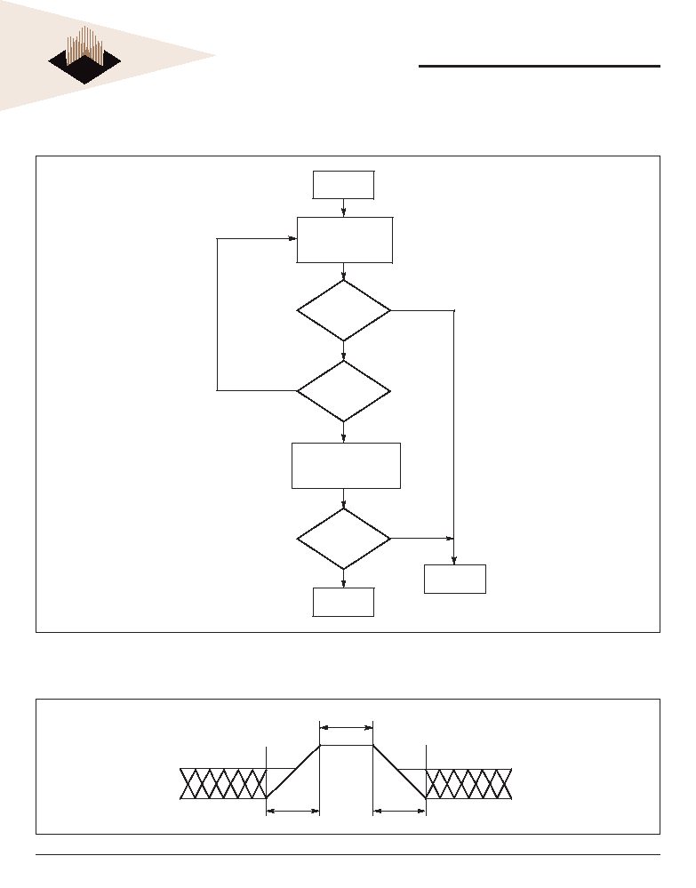
Figure 1 illustrates the Embedded Programming Algorithm
using typical command strings and bus operations.
CHIP ERASE
Chip erase is a six bus cycle operation. There are two
"unlock" write cycles. These are followed by writing the
"set-up" command. Two more "unlock" write cycles are
then followed by the chip erase command.
Chip erase does not require the user to program the
device prior to erase. Upon executing the Embedded
Erase Algorithm command sequence the device will
automatically program and verify the entire memory for an
all zero data pattern prior to electrical erase. The system
is not required to provide any controls or timings during
these operations.
The automatic erase begins on the rising edge of the last
WE# pulse in the command sequence and terminates
when the data on DQ7 is "1" (see Write Operation Status
section) at which time the device returns to read mode.
Figure 2 illustrates the Embedded Erase Algorithm using
typical command strings and bus operations.
SECTOR ERASE
Sector erase is a six bus cycle operation. There are two
"unlock" write cycles. These are followed by writing the
"set-up" command. Two more "unlock" write cycles are
then followed by the sector erase command. The sector
address (any address location within the desired sector)
is latched on the falling edge of WE#, while the command
(30h) is latched on the rising edge of WE#. After a time-
out of 50 µs from the rising edge of the last sector erase
command, the sector erase operation will begin.
Multiple sectors may be erased sequentially by writing
the six bus cycle operations as described above. This
sequence is followed with writes of the Sector Erase
command to addresses in other sectors desired to be
concurrently erased. The time between writes must be less
than 50 µs otherwise that command will not be accepted
and erasure will start. It is recommended that processor
interrupts be disabled during this time to guarantee this
condition. The interrupts can be re-enabled after the last
Sector Erase command is written. A time-out of 50 µs from
the rising edge of the last WE# will initiate the execution
of the Sector Erase command(s). If another falling edge
of the WE# occurs within the 50 µs time-out window the
timer is reset. (Monitor DQ3 to determine if the sector
erase timer window is still open, see section DQ3, Sector
Erase Timer.) Any command other than Sector Erase or
Erase Suspend during this period will reset the device to
the read mode, ignoring the previous command string. In
that case, restart the erase on those sectors and allow
them to complete.(Refer to the Write Operation Status
section for DQ3, Sector Erase Timer, operation.) Loading
the sector erase buffer may be done in any sequence and
with any number of sectors (0 to 31).
Sector erase does not require the user to program the
device prior to erase. The device automatically programs
all memory locations in the sector(s) to be erased prior
to electrical erase. When erasing a sector or sectors the
remaining unselected sectors are not affected. The system
is not required to provide any controls or timings during
these operations.
The automatic sector erase begins after the 50 µs time out
from the rising edge of the WE# pulse for the last sector
erase command pulse and terminates when the data on

10
White Electronic Designs Corporation ∑ (602) 437-1520 ∑ www.wedc.com
White Electronic Designs
EDI7F292MC
EDI7F492MC
January 2006
Rev. 1
PRELIMINARY
DQ7, Data# Polling, is "1" (see Write Operation Status
section) at which time the device returns to the read mode.
Data# Polling must be performed at an address within any
of the sectors being erased.
Figure 2 illustrates the Embedded Erase Algorithm using
typical command strings and bus operations.
ERASE SUSPEND
The Erase Suspend command allows the user to interrupt
a Sector Erase operation and then perform data reads or
programs to a sector not being erased. This command is
applicable ONLY during the Sector Erase operation which
includes the time-out period for sector erase. The Erase
Suspend command will be ignored if written during the Chip
Erase operation or Embedded Program Algorithm. Writing
the Erase Suspend command during the Sector Erase
time-out results in immediate termination of the time-out
period and suspension of the erase operation.
Any other command written during the Erase Suspend
mode will be ignored except the Erase Resume command.
Writing the Erase Resume command resumes the erase
operation. The addresses are "don't-cares" when writing
the Erase Suspend or Erase Resume command.
When the Erase Suspend command is written during the
Sector Erase operation, the device will take a maximum
of 15 µs to suspend the erase operation. When the device
has entered the erase-suspended mode, the RY/BY#
output pin and the DQ7 bit will be at logic `1', and DQ6
will stop toggling. The user must use the address of the
erasing sector for reading DQ6 and DQ7 to determine if
the erase operation has been suspended. Further writes
of the Erase Suspend command are ignored.
When the erase operation has been suspended, the device
defaults to the erase-suspend-read mode. Reading data in
this mode is the same as reading from the standard read
mode except that the data must be read from sectors that
have not been erase-suspended. Successively reading
from the erase-suspended sector while the device is in
the erase-suspend-read mode will cause DQ2 to toggle.
(See the section on DQ2).
After entering the erase-suspend-read mode, the user can
program the device by writing the appropriate command
sequence for Byte Program. This program mode is
known as the erase-suspend-program mode. Again,
programming in this mode is the same as programming in
the regular Byte Program mode except that the data must
be programmed to sectors that are not erase-suspended.
Successively reading from the erase-suspended sector
while the device is in the erase-suspend-program mode
will cause DQ2 to toggle. The end of the erase-suspended
program operation is detected by the RY/BY# output pin,
Data# Polling of DQ7, or by the Toggle Bit I (DQ6) which
is the same as the regular Byte Program operation. Note
that DQ7 must be read from the byte program address
while DQ6 can be read from any address.
To resume the operation of Sector Erase, the Resume
command (30h) should be written. Any further writes of the
Resume command at this point will be ignored. Another
Erase Suspend command can be written after the chip
has resumed erasing.

11
White Electronic Designs Corporation ∑ (602) 437-1520 ∑ www.wedc.com
White Electronic Designs
EDI7F292MC
EDI7F492MC
January 2006
Rev. 1
PRELIMINARY
TABLE 6. WRITE OPERATION STATUS
In Progress
Status
DQ7
CQ6
DQ5
DQ3
DQ2
Byte Program in Embedded Program Algorithm
DQ7#
Toggle
0
0
1
Embedded Program Algorithm
0
Toggle
0
1
Toggle
Erase Suspended Mode
Erase Suspended Read
(Erase Suspended Sector)
1
1
0
1
Toggle
(Note 1)
Erase Suspended Read
(Non-Erase Suspended Sector)
Data
Data
Data
Data
Data
Erase Suspended Read
(Non-Erase Suspended Sector)
DQ7#
Toggle
(Note 2)
0
1
1
(Note 3)
Exceeded Time
Limits
Byte Program in Embedded Program Algorithm
DQ7#
Toggle
1
0
1
Program/Erase Program in Embedded Program Algorithm
0
Toggle
1
1
N/A
Erase Suspended Mode
Erase Suspended Read
(Non-Erase Suspended Sector)
DQ7#
Toggle
1
1
N/A
Notes:
1.
Performing successive read operations from the erase-suspended sector will cause DQ2 to toggle.
2.
Performing successive read operations from any address will cause DQ6 to toggle.
3.
Reading the byte address being programmed while in the erase-suspend program mode will indicate logic `1' at the DQ2 bit.
However, successive reads from the erase-suspended sector will cause DQ2 to toggle.
DQ7
DATA# POLLING
The EDI7F292/492MC device features Data# Polling
as a method to indicate to the host that the embedded
algorithms are in progress or completed. During the
Embedded Program Algorithm, an attempt to read the
device will produce the complement of the data last written
to DQ7. Upon completion of the Embedded Program
Algorithm, an attempt to read the device will produce the
true data last written to DQ7. During the Embedded Erase
Algorithm, an attempt to read the device will produce a
"0" at the DQ7 output. Upon completion of the Embedded
Erase Algorithm an attempt to read the device will produce
a "1" at the DQ7 output. The fl owchart for Data# Polling
(DQ7) is shown in Figure 3.
Data# Polling will also fl ag the entry into Erase Suspend.
DQ7 will switch "0" to "1" at the start of the Erase Suspend
mode. Please note that the address of an erasing sector
must be applied in order to observe DQ7 in the Erase
Suspend Mode.
During Program in Erase Suspend, Data# Polling will
perform the same as in regular program execution outside
of the suspend mode.
For chip erase, the Data# Polling is valid after the
rising edge of the sixth WE# pulse in the six write pulse
sequence. For sector erase, the Data# Polling is valid after
the last rising edge of the sector erase WE# pulse. Data#
Polling must be performed at sector addresses within any
of the sectors being erased and not a sector that is within
a protected sector group. Otherwise, the status may not
be valid.
Just prior to the completion of Embedded Algorithm
operations DQ7 may change asynchronously while the
output enable (OE#) is asserted low. This means that the
device is driving status information on DQ7 at one instant
of time and then that byte's valid data at the next instant
of time. Depending on when the system samples the DQ7
output, it may read the status or valid data. Even if the
device has completed the Embedded Algorithm operations
and DQ7 has a valid data, the data outputs on DQ0≠DQ6
may be still invalid. The valid data on DQ0≠DQ7 can be
read on the successive read attempts.
The Data# Polling feature is only active during the
Embedded Programming Algorithm, Embedded Erase
Algorithm, Erase Suspend, erase-suspend-program mode,
or sector erase time-out (see Table 6).
See Figure 11 for the Data# Polling timing specifi cations
and diagrams.

12
White Electronic Designs Corporation ∑ (602) 437-1520 ∑ www.wedc.com
White Electronic Designs
EDI7F292MC
EDI7F492MC
January 2006
Rev. 1
PRELIMINARY
DQ6
TOGGLE BIT I
The EDI7F292/492MC also features the "Toggle Bit I" as a
method to indicate to the host system that the embedded
algorithms are in progress or completed.
During an Embedded Program or Erase Algorithm cycle,
successive attempts to read (OE# toggling) data from the
device at any address will result in DQ6 toggling between
one and zero. Once the Embedded Program or Erase
Algorithm cycle is completed, DQ6 will stop toggling and
valid data will be read on the next successive attempts.
During programming, the Toggle Bit I is valid after the
rising edge of the fourth WE# pulse in the four write pulse
sequence. For chip erase, the Toggle Bit I is valid after the
rising edge of the sixth WE# pulse in the six write pulse
sequence. For Sector Erase, the Toggle Bit I is valid after
the last rising edge of the sector erase WE# pulse. The
Toggle Bit I is active during the sector erase time out.
Either CS# or OE# toggling will cause the DQ6 to toggle.
In addition, an Erase Suspend/Resume command will
cause DQ6 to toggle. See Figure 12 for the Toggle Bit I
timing specifi cations and diagrams.
DQ5
EXCEEDED TIMING LIMITS
DQ5 will indicate if the program or erase time has
exceeded the specifi ed limits (internal pulse count). Under
these conditions DQ5 will produce a "1". This is a failure
condition which indicates that the program or erase cycle
was not successfully completed. Data# Polling is the only
operating function of the device under this condition. The
CS# circuit will partially power down the device under these
conditions (to approximately 2 mA). The OE# and WE#
pins will control the output disable functions as described
in Table 1.
The DQ5 failure condition will also appear if a user tries to
program a "1" to a location that is previously programmed
to "0". In this case the device locks out and never
completes the Embedded Program Algorithm. Hence, the
system never reads a valid data on DQ7 bit and DQ6 never
stops toggling. Once the device has exceeded timing limits,
the DQ5 bit will indicate a "1." Please note that this is not
a device failure condition since the device was incorrectly
used. If this occurs, reset the device.
DQ3
SECTOR ERASE TIMER
After the completion of the initial sector erase command
sequence the sector erase time-out will begin. DQ3 will
remain low until the time-out is complete. Data# Polling
and Toggle Bit I are valid after the initial sector erase
command sequence. If Data# Polling or the Toggle Bit I
indicates the device has been written with a valid erase
command, DQ3 may be used to determine if the sector
erase timer window is still open. If DQ3 is high ("1") the
internally controlled erase cycle has begun; attempts to
write subsequent commands (other than Erase Suspend)
to the device will be ignored until the erase operation is
completed as indicated by Data# Polling or Toggle Bit I. If
DQ3 is low ("0"), the device will accept additional sector
erase commands. To insure the command has been
accepted, the system software should check the status of
DQ3 prior to and following each subsequent sector erase
command. If DQ3 were high on the second status check,
the command may not have been accepted.
Refer to Table 6: Write Operation Status.
DQ2
TOGGLE BIT II
This toggle bit, along with DQ6, can be used to determine
whether the device is in the Embedded Erase Algorithm
or in Erase Suspend.
Successive reads from the erasing sector will cause DQ2
to toggle during the Embedded Erase Algorithm. If the
device is in the erase-suspended-read mode, successive
reads from the erase-suspend sector will cause DQ2
to toggle. When the device is in the erase-suspended-
program mode, successive reads from the byte address
of the non-erase suspended sector will indicate a logic `1'
at the DQ2 bit.
DQ6 is different from DQ2 in that DQ6 toggles only
when the standard Program or Erase, or Erase Suspend
Program operation is in progress. The behavior of these
two status bits, along with that of DQ7, is summarized as
follows:
13
White Electronic Designs Corporation ∑ (602) 437-1520 ∑ www.wedc.com
White Electronic Designs
EDI7F292MC
EDI7F492MC
January 2006
Rev. 1
PRELIMINARY
Mode
DQ7
DQ6
DQ2
Program
DQ7#
toggles
1
Erase
0
toggles
toggles
Erase Suspend Read (1)
(Erase-Suspend Sector)
1
1
toggles
Erase Suspend Program
DQ7# (2)
toggles
1 (2)
Notes:
1.
These status fl ags apply when outputs are read from a sector that has been
erase-suspended.
2.
These status fl ags apply when outputs are read from the byte address of the
non-erase suspended sector.
For example, DQ2 and DQ6 can be used together to
determine the erase-suspend-read mode (DQ2 toggles
while DQ6 does not). See also Table 6 and Figure 17.
Furthermore, DQ2 can also be used to determine which
sector is being erased. When the device is in the erase
mode, DQ2 toggles if this bit is read from the erasing
sector.
RY/BY#
READY/BUSY#
The EDI7F292/492MC provides a RY/BY# open-drain
output pin as a way to indicate to the host system that
the Embedded Algorithms are either in progress or has
been completed. If the output is low, the device is busy
with either a program or erase operation. If the output is
high, the device is ready to accept any read/write or erase
operation. When the RY/BY# pin is low, the device will
not accept any additional program or erase commands
with the exception of the Erase Suspend command. If the
EDI7F292/492MC is placed in an Erase Suspend mode,
the RY/BY# output will be high.
During programming, the RY/BY# pin is driven low after
the rising edge of the fourth WE# pulse. During an erase
operation, the RY/BY# pin is driven low after the rising
edge of the sixth WE# pulse. The RY/BY# pin will indicate
a busy condition during the RESET# pulse. Refer to Figure
13 for a detailed timing diagram. The RY/BY# pin is pulled
high in standby mode.
Since this is an open-drain output, several RY/BY# pins
can be tied together in parallel with a pull-up resistor to
V
CC
.
RESET#
HARDWARE RESET
The EDI7F292/492MC device may be reset by driving the
RESET# pin to V
IL
. The RESET# pin must be kept low
(V
IL
) for at least 500 ns. Any operation in progress will be
terminated and the internal state machine will be reset to
the read mode 20 µs after the RESET# pin is driven low.
If a hardware reset occurs during a program operation, the
data at that particular location will be indeterminate.
When the RESET# pin is low and the internal reset is
complete, the device goes to standby mode and cannot
be accessed. Also, note that all the data output pins are
tri-stated for the duration of the RESET# pulse. Once
the RESET# pin is taken high, the device requires
500 ns of wake up time until outputs are valid for read
access. The RESET# pin may be tied to the system
reset input. Therefore, if a system reset occurs during the
Embedded Program or Erase Algorithm, the device will
be automatically reset to read mode and this will enable
the system's microprocessor to read the boot-up fi rmware
from the Flash memory.
DATA PROTECTION
The EDI7F292/492MC is designed to offer protection
against accidental erasure or programming caused by
spurious system level signals that may exist during power
transitions. During power up the device automatically
resets the internal state machine in the Read mode. Also,
with its control register architecture, alteration of the
memory contents only occurs after successful completion
of specifi c multi-bus cycle command sequences.
The device also incorporates several features to prevent
inadvertent write cycles resulting from V
CC
power-up and
power-down transitions or system noise.
LOW V
CC
WRITE INHIBIT
To avoid initiation of a write cycle during V
CC
power-up and
power-down, a write cycle is locked out for V
CC
less than
3.2 V (typically 3.7 V). If V
CC
< V
LKO
, the command register
is disabled and all internal program/erase circuits are
disabled. Under this condition the device will reset to the
read mode. Subsequent writes will be ignored until the V
CC
level is greater than V
LKO
. It is the user's responsibility to
ensure that the control pins are logically correct to prevent
unintentional writes when V
CC
is above 3.2 V.

14
White Electronic Designs Corporation ∑ (602) 437-1520 ∑ www.wedc.com
White Electronic Designs
EDI7F292MC
EDI7F492MC
January 2006
Rev. 1
PRELIMINARY
WRITE PULSE "GLITCH" PROTECTION
Noise pulses of less than 5 ns (typical) on OE#, CS# or
WE# will not initiate a write cycle.
LOGICAL INHIBIT
Writing is inhibited by holding any one of OE# = V
IL
, CS#
=V
IH
or WE# = V
IH
. To initiate a write cycle CS# and WE#
must be a logical zero while OE# is a logical one.
POWER-UP WRITE INHIBIT
Power-up of the device with WE# = CS# = V
IL
, and OE#
= V
IH
will not accept command on the rising edge of WE#
The internal state machine is automatically reset to the
read mode on power-up.
FIGURE 1. EMBEDDED PROGRAMMING ALGORITHM
Start
Programming Completed
Last Address
?
Write Program Command Sequence
(see below)
Data# Poll Device
Increment Address
Yes
No
5555h/AAh
2AAAh/55h
5555h/A0h
Program Address/Program Data
Program Command Sequence (Address/Command):

15
White Electronic Designs Corporation ∑ (602) 437-1520 ∑ www.wedc.com
White Electronic Designs
EDI7F292MC
EDI7F492MC
January 2006
Rev. 1
PRELIMINARY
NOTE:
To insure the command has been accepted, the system software should check the status of DQ3 prior to and following each subsequent sector erase command. If DQ3 were high on
the second status check, the command may not have been accepted.
FIGURE 2. EMBEDDED ERASE ALGORITHM
Start
Erasure Completed
Write Erase Command Sequence
(see below)
Data# Polling or Toggle Bit I
Successfully Completed
5555h/AAh
2AAAh/55h
5555h/80h
Chip Erase Command Sequence
(Address/Command):
5555h/AAh
2AAAh/55h
5555h/10h
5555h/AAh
2AAAh/55h
5555h/80h
Individual Sector/Multiple Sector
Erase Command Sequence
(Address/Command):
5555h/AAh
Sector Address/30h
Sector Address/30h
Sector Address/30h
2AAAh/55h
Additional sector
erase commands
are optional

16
White Electronic Designs Corporation ∑ (602) 437-1520 ∑ www.wedc.com
White Electronic Designs
EDI7F292MC
EDI7F492MC
January 2006
Rev. 1
PRELIMINARY
FIGURE 3 DATA# POLLING ALGORITHM
Start
Fail
No
Yes
DQ7 = Data
?
No
Pass
Yes
No
Yes
DQ7 = Data
?
DQ5 = 1
?
Yes
Read Byte
(DQ0≠DQ7)
Addr = VA
Read Byte
(DQ0≠DQ7)
Addr = VA
FIGURE 5 MAXIMUM NEGATIVE OVERSHOOT WAVEFORM
20 ns
20 ns
+0.8 V
≠0.5 V
20 ns
≠2.0 V
VA = Byte address for programming
= Any of the sector addresses within the sector being
erased during sector erase operation
= Valid address equals any non-protected sector group
address during chip erase
DQ7 is rechecked even if DQ5 = "1" because DQ7 may change simultaneously with DQ5.
17
White Electronic Designs Corporation ∑ (602) 437-1520 ∑ www.wedc.com
White Electronic Designs
EDI7F292MC
EDI7F492MC
January 2006
Rev. 1
PRELIMINARY
FIGURE 4 TOGGLE BIT I ALGORITHM
Start
Fail
No
Yes
DQ6 = Toggle
?
Pass
Yes
No
Yes
DQ6 = Toggle
?
DQ5 = 1
?
Yes
Read Byte
(DQ0≠DQ7)
Addr = Don't Care
Read Byte
(DQ0≠DQ7)
Addr = Don't Care
No
FIGURE 6 MAXIUM POSITIVE OVERSHOOT WAVEFORM
20 ns
V
CC
+ 0.5 V
2.0 V
20 ns
20 ns
V
CC
+ 2.0 V
DQ6 is rechecked even if DQ5 = "1" because DQ6 may stop toggling at the same time as DQ5 changing to "1".

18
White Electronic Designs Corporation ∑ (602) 437-1520 ∑ www.wedc.com
White Electronic Designs
EDI7F292MC
EDI7F492MC
January 2006
Rev. 1
PRELIMINARY
Storage Temperature
Plastic Packages .................................. ≠65∞C to +150∞C
Ambient Temperature
with Power Applied ............................... ≠65∞C to +125∞C
Voltage with Respect to Ground
V
CC
(Note 1) ...................................... ≠2.0 V to +7.0 V
A9, OE#, and RESET# (Note 2) ...... ≠2.0 V to +13.5 V
All other pins (Note 1) ........................ ≠2.0 V to +7.0 V
Output Short Circuit Current (Note 3) ................. 200 mA
ABSOLUTE MAXIMUM RATINGS
Notes:
1.
Minimum DC voltage on input or I/O pins is ≠0.5 V. During voltage transitions,
input may overshoot V
SS
to ≠2.0 V for periods of up to 20 ns. Maximum DC
voltage on input or I/O pins is V
CC
+0.5 V. During voltage transitions, input or I/O
pins may overshoot to V
CC
+2.0 V for periods up to 20 ns. See Figure 8.
2.
Minimum DC input voltage on pins A9, OE#, and RESET# is -0.5 V. During
voltage transitions, A9, OE#, and RESET# may overshoot V
SS
to ≠2.0 V for
periods of up to 20 ns. Maximum DC input voltage on pin A9 is +12.5 V which
may overshoot to 14.0 V for periods up to 20 ns.
3.
No more than one output may be shorted to ground at a time. Duration of the
short circuit should not be greater than one second.
Stresses above those listed under "Absolute Maximum Ratings" may cause permanent
damage to the device. This is a stress rating only; functional operation of the device at
these or any other conditions above those indicated in the operational sections of this
data sheet is not implied. Exposure of the device to absolute maximum rating conditions
for extended periods may affect device reliability.
OPERATING RANGES
Commercial (C) Devices
Case Temperature (T
C
) .............................. 0∞C to +70∞C
Industrial (I) Devices
Case Temperature (T
C
) .......................... ≠40∞C to +85∞C
V
CC
Supply Voltages
V
CC
for EDI7F292/492MC ................ +4.75 V to +5.25 V
V
CC
for EDI7F292/492MC 100, 120 .. +4.50 V to +5.50 V
Operating ranges defi ne those limits between which the functionality of the device is
guaranteed.

19
White Electronic Designs Corporation ∑ (602) 437-1520 ∑ www.wedc.com
White Electronic Designs
EDI7F292MC
EDI7F492MC
January 2006
Rev. 1
PRELIMINARY
DC CHARACTERISTICS (EDI7F292MC)
TTL/NMOS COMPATIBLE
Parameter
Symbol
Parameter Description
Test Description
Min
Max
Units
I
LI
Input Load Current
V
IN
= V
SS
to V
CC
= V
CCMAX
±1.0
µA
I
LIT
A9 Input Load Current
V
CC
= V
CCMAX
, A9 = 12.0 Volt
50
µA
I
LO
Output Leakage Current
V
OUT
= V
SS
to V
CC
, V
CC
= V
CCMAX
±1.0
µA
I
CC1
V
CC
Active Current (Note 1)
CS# = V
IL
, OE# = V
IH
80
mA
I
CC2
V
CC
Active Current (Notes 2, 3)
CS# = V
IL
, OE# = V
IH
120
mA
I
CC3
V
CC
Standby Current
V
CC
= V
CCMAX
, CS# = V
IL
, RESET# = V
IH
2
mA
I
CC4
V
CC
Standby Current (Reset)
V
CC
= V
CCMAX
, RESET# = V
IL
2
mA
V
IL
Input Low Level
-0.5
0.8
mA
V
IH
Input High Level
2.0
V
CC
+ 0.5
V
V
ID
Voltage for Autoselect and
Sector Protect
V
CC
= 5.0 Volt
11.5
12.5
V
V
OL
Output Low Voltage
I
OL
= 12 mA V
CC
= V
CCMIN
0.45
V
V
OH
Output High Level
I
OH
= -2.5 mA V
CC
= V
CCMIN
2.4
V
V
LKO
Low V
CC
Lock-out Voltage
3.2
4.2
V
Notes:
1. The
I
CC
current listed includes both the DC operating current and the frequency dependent component (at 6 MHz). The frequency component typically is less than 1 mA/MHz,
with OE# at V
IH
.
2. I
CC
active while Embedded Program or Erase Algorithm is in progress.
3. Not
100%
tested.
DC CHARACTERISTICS (EDI7F292MC)
CMOS COMPATIBLE
Parameter
Symbol
Parameter Description
Test Description
Min
Typ
Max
Units
I
LI
Input Load Current
V
IN
= V
SS
to V
CC
, V
CC
= V
CCMAX
±1.0
µA
I
LIT
A9 Input Load Current
V
CC
= V
CCMAX
, A9 = 12.0 Volt
50
µA
I
LO
Output Leakage Current
V
OUT
= V
SS
to V
CC
, V
CC
= V
CCMAX
±1.0
µA
I
CC1
V
CC
Active Current (Note 1)
CS# = V
IL
, OE# = V
IH
50
80
mA
I
CC2
V
CC
Active Current (Notes 2, 3)
CS# = V
IL
, OE# = V
IH
60
80
mA
I
CC3
V
CC
Standby Current
V
CC
= V
CCMAX
, CS# = V
CC
± 0.3 V, RESET#
= V
CC
± 0.3 V
2
10
mA
I
CC4
V
CC
Standby Current (Reset)
V
CC
= V
CCMAX
, RESET# = V
CC
± 0.3 V
2
10
mA
V
IL
Input Low Level
-0.5
0.8
mA
V
IH
Input High Level
0.7 X V
CC
V
CC
+ 0.3
V
V
ID
Voltage for Autoselect and
Sector Protect
V
CC
= 5.0 Volt
11.5
12.5
V
V
OL
Output Low Voltage
I
OL
= 12 mA V
CC
= V
CCMIN
0.85 V
CC
0.45
V
V
OH
Output High Level
I
OH
= -2.5 mA V
CC
= V
CCMIN
2.4
V
I
OH
= -100 µA, V
CC
= V
CCMIN
V
CC
- 0.4
V
V
LKO
Low V
CC
Lock-out Voltage
3.2
4.2
V
Notes:
1. The
I
CC
current listed includes both the DC operating current and the frequency dependent component (at 6 MHz). The frequency component typically is less than 1 mA/MHz,
with OE# at V
IH
.
2. I
CC
active while Embedded Program or Erase Algorithm is in progress.
3. Not
100%
tested.
20
White Electronic Designs Corporation ∑ (602) 437-1520 ∑ www.wedc.com
White Electronic Designs
EDI7F292MC
EDI7F492MC
January 2006
Rev. 1
PRELIMINARY
DC CHARACTERISTICS (EDI7F492MC)
TTL/NMOS COMPATIBLE
Parameter
Symbol
Parameter Description
Test Description
Min
Max
Units
I
LI
Input Load Current
V
IN
= V
SS
to V
CC
= V
CCMAX
±1.0
µA
I
LIT
A9 Input Load Current
V
CC
= V
CCMAX
, A9 = 12.0 Volt
50
µA
I
LO
Output Leakage Current
V
OUT
= V
SS
to V
CC
, V
CC
= V
CCMAX
±1.0
µA
I
CC1
V
CC
Active Current (Note 1)
CS# = V
IL
, OE# = V
IH
160
mA
I
CC2
V
CC
Active Current (Notes 2, 3)
CS# = V
IL
, OE# = V
IH
240
mA
I
CC3
V
CC
Standby Current
V
CC
= V
CCMAX
, CS# = V
IL
, RESET# = V
IH
4
mA
I
CC4
V
CC
Standby Current (Reset)
V
CC
= V
CCMAX
, RESET# = V
IL
4
mA
V
IL
Input Low Level
-0.5
0.8
mA
V
IH
Input High Level
2.0
V
CC
+ 0.5
V
V
ID
Voltage for Autoselect and
Sector Protect
V
CC
= 5.0 Volt
11.5
12.5
V
V
OL
Output Low Voltage
I
OL
= 12 mA V
CC
= V
CCMIN
0.45
V
V
OH
Output High Level
I
OH
= -2.5 mA V
CC
= V
CCMIN
2.4
V
V
LKO
Low V
CC
Lock-out Voltage
3.2
4.2
V
Notes:
1. The
I
CC
current listed includes both the DC operating current and the frequency dependent component (at 6 MHz). The frequency component typically is less than 1 mA/MHz,
with OE# at V
IH
.
2. I
CC
active while Embedded Program or Erase Algorithm is in progress.
3. Not
100%
tested.
DC CHARACTERISTICS (EDI7F492MC)
CMOS COMPATIBLE
Parameter
Symbol
Parameter Description
Test Description
Min
Typ
Max
Units
I
LI
Input Load Current
V
IN
= V
SS
to V
CC
, V
CC
= V
CCMAX
±1.0
µA
I
LIT
A9 Input Load Current
V
CC
= V
CCMAX
, A9 = 12.0 Volt
50
µA
I
LO
Output Leakage Current
V
OUT
= V
SS
to V
CC
, V
CC
= V
CCMAX
±1.0
µA
I
CC1
V
CC
Active Current (Note 1)
CS# = V
IL
, OE# = V
IH
100
160
mA
I
CC2
V
CC
Active Current (Notes 2, 3)
CS# = V
IL
, OE# = V
IH
120
160
mA
I
CC3
V
CC
Standby Current
V
CC
= V
CCMAX
, CS# = V
CC
± 0.3 V, RESET#
= V
CC
± 0.3 V
4
20
mA
I
CC4
V
CC
Standby Current (Reset)
V
CC
= V
CCMAX
, RESET# = V
CC
± 0.3 V
4
20
mA
V
IL
Input Low Level
-0.5
0.8
mA
V
IH
Input High Level
0.7 X V
CC
V
CC
+ 0.3
V
V
ID
Voltage for Autoselect and
Sector Protect
V
CC
= 5.0 Volt
11.5
12.5
V
V
OL
Output Low Voltage
I
OL
= 12 mA V
CC
= V
CCMIN
0.85 V
CC
0.45
V
V
OH
Output High Level
I
OH
= -2.5 mA V
CC
= V
CCMIN
2.4
V
I
OH
= -100 µA, V
CC
= V
CCMIN
V
CC
- 0.4
V
V
LKO
Low V
CC
Lock-out Voltage
3.2
4.2
V
Notes:
1. The
I
CC
current listed includes both the DC operating current and the frequency dependent component (at 6 MHz). The frequency component typically is less than 1 mA/MHz,
with OE# at V
IH
.
2. I
CC
active while Embedded Program or Erase Algorithm is in progress.
3. Not
100%
tested.
21
White Electronic Designs Corporation ∑ (602) 437-1520 ∑ www.wedc.com
White Electronic Designs
EDI7F292MC
EDI7F492MC
January 2006
Rev. 1
PRELIMINARY
AC CHARACTERISTICS
READ-ONLY OPERATIONS CHARACTERISTICS
Parameter Symbol
Parameter Desription
Test Setup
Speed Options (Notes 1 and 2)
JEDEC
Standard
-100
-120
t
AVAV
t
RC
Read Cycle Time 4
CS# = V
IL
OE# = V
IL
Min
100
120
t
AVQV
t
ACC
Address to Output Delay
OE# = V
IL
Max
100
120
t
ELQV
t
CS
Chip Enable to Output Delay
Max
100
120
t
GLQV
t
OE
Output Enable to Output Delay
Max
40
50
t
EHQZ
t
DF
Chip Enable to Output High Z (Notes 3, 4)
Max
20
30
t
GHQZ
t
DF
Output Enable to Output High Z (Notes 3, 4)
Max
20
30
t
AXQX
t
OH
Output Hold Time From Addresses CS# or
OE# Which Ever Occurs First
Min
0
0
t
Ready
RESET# Pin Low to Read Mode 4
Max
20
20
Notes:
1.
Test Conditions (for all others): Output Load: 1 TTL gate and 100 pF Input rise and fall times: 20 ns Input pulse levels: 0.45 V to 2.4 V Timing measurement reference level: 0.8 V
and 2.0 V input and output.
2.
Output driver disable time.
3. Not
100%
tested.
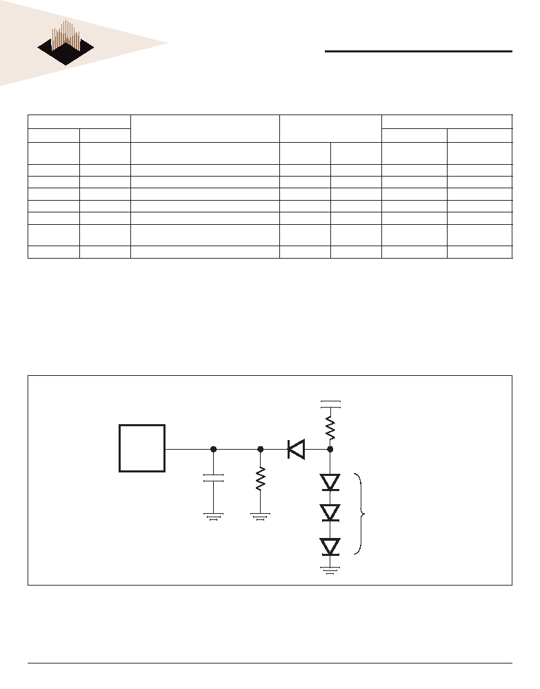
FIGURE 7 TEST CONDITIONS
2.7 k
Diodes = 1N3064
or Equivalent
C
L
6.2 k
5.0 Volt
1N3064
or Equivalent
Device
Under
Test
Note:
CL = 100 pF including jig capacitance

22
White Electronic Designs Corporation ∑ (602) 437-1520 ∑ www.wedc.com
White Electronic Designs
EDI7F292MC
EDI7F492MC
January 2006
Rev. 1
PRELIMINARY
AC CHARACTERISTICS
WRITE/ERASE/PROGRAM OPERATIONS
Parameter Symbol
Parameter Desription
Speed Options (Notes 1 and 2)
JEDEC
Standard
-100
-120
t
AVAV
t
WC
Write Cycle Time
Min
100
120
t
AVWL
t
AS
Address Setup Time
Min
0
0
t
WLAX
t
AH
Address Hold Time
Min
45
50
t
DVWH
t
DS
Data Setup Time
Min
45
50
t
WHDX
t
DH
Data Hold Time
Min
0
0
t
OEH
Output Enable Hold
Time
Read 2
Min
0
0
Toggle Bit I and
Data# Polling 2
Min
10
10
t
GHWL
t
GHWL
Read Recover Time Before Write OE# high to
WE# low
Min
0
0
t
ELWL
t
CS
CS# Setup Time
Min
0
0
t
WHEH
t
CH
CS# Hold Time
Min
0
0
t
WLWH
t
WP
Write Pulse Width
Min
45
50
t
WHWL
t
WPH
Write Pulse Width High
Min
20
20
t
WHWH1
t
WHWH1
Byte Programming Operation
Typ
7
7
t
WHWH2
t
WHWH2
Sector Erase Operation 1
Typ
1
1
Max
8
8
t
VCS
V
CC
Set Up Time 2
Min
50
50
t
VIDR
Rise Time to VID (Notes 2, 3)
Min
500
500
t
VLHT
Voltage Transition Time (Notes 2, 3)
Min
4
4
t
OESP
OE# Setup Time to WE# Active ( 2, 3)
Min
4
4
t
RP
RESET# Pulse Width
Min
500
500
t
BUSY
Program/Erase Valid to RY/BY# Delay
Min
40
50
Notes:
1.
This does not include the preprogramming time.
2. Not
100%
tested.
3.
These timings are for Temporary Sector Group Unprotect operation.

23
White Electronic Designs Corporation ∑ (602) 437-1520 ∑ www.wedc.com
White Electronic Designs
EDI7F292MC
EDI7F492MC
January 2006
Rev. 1
PRELIMINARY
SWITCHING TEST WAVEFORM
KEY TO SWITCHING WAVEFORMS
Must be
Steady
May
Change
from H to L
May
Change
from L to H
Does Not
Apply
Don't Care,
Any Change
Permitted
Will be
Steady
Will be
Changing
from H to L
Will be
Changing
from L to H
Changing,
State
Unknown
Center
Line is High-
Impedance
"Off" State
WAVEFORM
INPUTS
OUTPUTS
Addresses
CS#
OE#
WE#
Outputs
Addresses Stable
High Z
High Z
(t
DF
)
(t
CE
)
(t
OH
)
Output Valid
t
ACC
t
OE
t
RC
t
OEH
FIGURE 8. AC WAVEFORM FOR READ OPERATION

24
White Electronic Designs Corporation ∑ (602) 437-1520 ∑ www.wedc.com
White Electronic Designs
EDI7F292MC
EDI7F492MC
January 2006
Rev. 1
PRELIMINARY
SWITCHING WAVEFORMS
FIGURE 9. PROGRAM OPERATION TIMINGS
D
OUT
PD
t
AH
t
RC
Data# Polling
t
DF
t
OH
t
CE
t
OE
t
DS
t
CS
t
WPH
t
DH
t
WP
t
GHWL
Addresses
CE#
OE
WE#
Data
5.0 Volt
t
WC
t
AS
DQ7
5555H
PA
A0H
t
WHWH1
PA
3rd Bus Cycle
Notes:
1.
PA is address of the memory location to be programmed.
2.
PD is data to be programmed at byte address.
3.
DQ7# is the output of the complement of the data written to the device.
4. D
OUT
is the output of the data written to the device.
5.
Figure indicates last two bus cycles of four bus cycle sequence.
FIGURE 10. AC WAVEFORMS CHIP/SECTOR ERASE OPERATIONS
t
AH
t
AS
t
WP
t
CS
t
DH
5555H
2AAAH
SA
CS#
OE#
WE#
Data
V
CC
AAH
55H
80H
AAH
55H
10H/30H
t
WPH
Addresses
2AAAH
t
VCS
t
DS
5555H
t
GHWL
5555H
Notes:
1.
SA is the sector address for Sector Erase. Addresses = don't care for Chip Erase.

25
White Electronic Designs Corporation ∑ (602) 437-1520 ∑ www.wedc.com
White Electronic Designs
EDI7F292MC
EDI7F492MC
January 2006
Rev. 1
PRELIMINARY
SWITCHING WAVEFORMS
FIGURE 11. AC WAVEFORMS FOR DATA# POLLING DURING EMBEDDED
ALGORITHM OPERATION
FIGURE 12. AC WAVEFORMS FOR TOGGLE BIT I DURING EMBEDDED
ALGORITHM OPERATIONS
DQ0≠DQ7
Valid Data
t
CH
t
OEH
t
OE
t
CE
t
WHWH 1 or 2
DQ7 =
Valid Data
High Z
CS#
OE#
WE#
DQ7
t
OH
t
DF
DQ7
DQ0≠DQ6
DQ0≠DQ6 = Invalid
*
Notes:
DQ7 = Valid Data (The device has completed the Embedded operation).
CS#
t
OEH
WE#
OE#
DQ6 =
Stop Toggling
DQ0≠DQ7
Valid
DQ6 = Toggle
DQ6 = Toggle
Data (DQ0≠DQ7)
*
t
OE
Notes:
∑ DQ6 stops toggling (The device has completed the Embedded operation).

26
White Electronic Designs Corporation ∑ (602) 437-1520 ∑ www.wedc.com
White Electronic Designs
EDI7F292MC
EDI7F492MC
January 2006
Rev. 1
PRELIMINARY
FIGURE 14. RESET# TIMING DIAMGRAM
FIGURE 13. BY/RY# TIMING DIAGRAM DURING PROGRAM/ERASE OPERATIONS
CS#
WE#
RY/BY#
t
BUSY
Entire programming
or erase operations
The rising edge of the last WE# signal
Start
Perform Erase or
Program Operations
RESET# = V
IH
Temporary Sector Group
Unprotect Completed
(Note 2)
RESET# = V
ID
(Note 1)
RESET#
t
Ready
t
RP
FIGURE 15. TEMPORARY SECTOR GROUP UNPORTECT ALGORITHM
Notes:
1.
All protected sector groups unprotected.
2.
All previously protected sector groups are protected once
again.

27
White Electronic Designs Corporation ∑ (602) 437-1520 ∑ www.wedc.com
White Electronic Designs
EDI7F292MC
EDI7F492MC
January 2006
Rev. 1
PRELIMINARY
FIGURE 16. TEMPORARY SECTOR GROUP UNPORTECT TIMING DIAMGRAM
RY/BY#
Program or Erase Command Sequence
RESET#
CS#
WE#
0V or 5 V
0 or 5V
t
VIDR
12V
FIGURE 17. DQ2 VS. DQ6
Enter
Erase
Erase
Erase
Enter Erase
Suspend Program
Erase Suspend
Read
Erase Suspend
Read
Erase
WE#
DQ6
DQ2
Toggle
DQ2 and DQ6
with OE#
Erase
Complete
Erase
Suspend
Suspend
Program
Resume
Embedded
Erasing
Notes:
∑ DQ2 is read from the erase-suspended sector.
28
White Electronic Designs Corporation ∑ (602) 437-1520 ∑ www.wedc.com
White Electronic Designs
EDI7F292MC
EDI7F492MC
January 2006
Rev. 1
PRELIMINARY
AC CHARACTERISTICS
WRITE/ERASE/PROGRAM OPERATIONS
Alternate CS# Controlled Writes
Parameter Symbol
Parameter Desription
Speed Options (Notes 1 and 2)
JEDEC
Standard
-100
-120
t
AVAV
t
WC
Write Cycle Time
Min
100
120
t
AVWL
t
AS
Address Setup Time
Min
0
0
t
WLAX
t
AH
Address Hold Time
Min
45
50
t
DVWH
t
DS
Data Setup Time
Min
45
50
t
WHDX
t
DH
Data Hold Time
Min
0
0
t
OEH
Output Enable Hold
Time
Read (Note 2)
Min
0
0
Toggle Bit I and
Data# Polling
(Note 2)
Min
10
10
t
GHWL
t
GHWL
Read Recover Time Before Write OE# high to
WE# low
Min
0
0
t
ELWL
t
CS
CS# Setup Time
Min
0
0
t
WHEH
t
CH
CS# Hold Time
Min
0
0
t
WLWH
t
WP
Write Pulse Width
Min
45
50
t
WHWL
t
WPH
Write Pulse Width High
Min
20
20
t
WHWH1
t
WHWH1
Byte Programming Operation
Typ
7
7
t
WHWH2
t
WHWH2
Sector Erase Operation (Note 1)
Typ
1
1
Max
8
8
Notes:
1.
This does not include the preprogramming time.
2. Not
100%
tested.

29
White Electronic Designs Corporation ∑ (602) 437-1520 ∑ www.wedc.com
White Electronic Designs
EDI7F292MC
EDI7F492MC
January 2006
Rev. 1
PRELIMINARY
FIGURE 18. ALTERNATE CS# CONTROLLED PROMGRAM OPERATION TIMING
D
OUT
PD
t
AH
Data# Polling
t
DS
t
WS
t
CPH
t
DH
t
CP
t
GHEL
Addresses
WE#
OE#
CS#
Data
5.0 Volt
t
WC
t
AS
DQ7#
5555H
PA
A0H
t
WHWH1
PA
Notes:
1.
PA is address of the memory location to be programmed.
2.
PD is data to be programmed at byte address.
3.
DQ7# is the output of the complement of the data written to the device.
4. D
OUT
is the output of the data written to the device.
5.
Figure indicates last two bus cycles of four bus cycle sequence.
ERASE AND PROGRAMMING PERFORMANCE
Parameter
Limits
Unit
Comments
Min
Typ
Max
Sector Erase Time
1 (Note 1)
8
sec
Excludes 00H programming prior to erasure
Chip Erase Time
32
256
sec
Excludes 00H programming prior to erasure
Byte Programming Time
7
300 ( Note 3)
µs
Excludes system-level overhead
Chip Programming Time
14.4 (Note 1)
43.2 (Notes 2, 3)
sec
Excludes system-level overhead
Notes:
1.
25∞C, 5V V
CC
, 100,000 cycles.
2.
Although Embedded Algorithms allow for a longer chip program and erase time, the actual time will be considerably less since bytes program or erase signifi cantly faster than the
worst case byte.
3.
Under worst case condition of 90∞C, 4.5 V V
CC
, 100,000 cycles.

30
White Electronic Designs Corporation ∑ (602) 437-1520 ∑ www.wedc.com
White Electronic Designs
EDI7F292MC
EDI7F492MC
January 2006
Rev. 1
PRELIMINARY
LATCHUP CHARACTERISTIC
Min
Max
Input Voltage with respect to V
SS
on I/O pin
-1.0 V
V
CC
+ 1.0 V
V
CC
Current
-100mA
+100 mA
Notes:
∑ Includes all pins except V
CC
. Test conditions: V
CC
= 5.0 Volt, one pin at a time.
CAPACITANCE
(f = 1.0 MHz, V
IN
= V
CC
or V
SS
)
Parameter
Sym
2x2xMx8
4x2Mx8
Unit
Max
Max
Address Lines
CA
20
35
pF
Data Lines
CDQ
30
50
pF
Chip & Write Enable Lines
CC
12
12
pF
Output Enable Lines
CG
20
40
pF
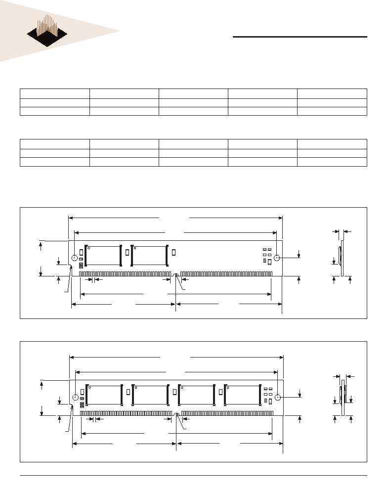
31
White Electronic Designs Corporation ∑ (602) 437-1520 ∑ www.wedc.com
White Electronic Designs
EDI7F292MC
EDI7F492MC
January 2006
Rev. 1
PRELIMINARY
ORDERING IN FOR MA TION
EDI7292MC
5.72
(0.225)
MIN
3.18
(0.125)
MIN
3.05
(0.120)
MAX
J1
J3
153
1.57
(0.062) R
1.57 (0.062) R
21.59
(0.850)
MAX
118.24
(4.655) MAX.
111.35
(4.384)
6.35
(0.250)
57.02
(2.245)
55.68
(2.192)
10.16
(0.400)
105.41
(4.150)
1.27
(0.050) TYP
6.35 (0.250)
R3
R1
EDI7292MC
Part Num ber
Speed (ns)
Pack age
T
A
Commercial Range
Height*
EDI7292MC100BNC
100
361
0∞C to +70∞C
21.59 (0.850")
EDI7292MC120BNC
120
361
0∞C to +70∞C
21.59 (0.850")
EDI7492MC
Part Num ber
Speed (ns)
Pack age
T
A
Industrial Range
Height*
EDI7492MC100BNI
100
361
0∞C to +70∞C
21.59 (0.850")
EDI7492MC120BNI
120
361
0∞C to +70∞C
21.59 (0.850")
Notes:
∑ Consult factors for availability of lead-free or RoHS products.
∑ Consult factors for availability of industrail temp (-40∞C to 85∞C) option.
* ALL DIMENSIONS ARE IN MILLIMETERS AND (INCHES)
EDI7492MC
5.72
(0.225)
MIN
3.18
(0.125)
MIN
4.32
(0.170)
MAX
J1
J3
153
1.57
(0.062) R
1.57 (0.062) R
21.59
(0.850)
MAX
118.24
(4.655) MAX.
111.35
(4.384)
6.35
(0.250)
57.02
(2.245)
55.68
(2.192)
10.16
(0.400)
105.41
(4.150)
1.27
(0.050) TYP
6.35 (0.250)
R3
R1
* ALL DIMENSIONS ARE IN MILLIMETERS AND (INCHES)

32
White Electronic Designs Corporation ∑ (602) 437-1520 ∑ www.wedc.com
White Electronic Designs
EDI7F292MC
EDI7F492MC
January 2006
Rev. 1
PRELIMINARY
PART NUMBERING GUIDE
EDI 7 F 292M/492M C xxx BN X
WEDC
FLASH
FR4 WITH TIN LEAD CONTACTS
MODULE BUS WIDTH: x8
VOLTAGE; 5V (CMOS)
SPEED: 100, 120ns
PACKAGE: 80 Pin SIMM
TEMPERATURE RANGE
C = 0∞C to 70∞C Commercial
I = -40∞C to 85∞C Industrial

33
White Electronic Designs Corporation ∑ (602) 437-1520 ∑ www.wedc.com
White Electronic Designs
EDI7F292MC
EDI7F492MC
January 2006
Rev. 1
PRELIMINARY
Document Title
4MB/8MB Flash Module (2x2Mx8) & (4x2Mx8)
Revision History
Rev #
History
Release Date
Status
Rev 0
Created
5-02
Advanced
Rev 1
Updated datasheet
1-06
Final