1
White Electronic Designs Corporation ∑ (602) 437-1520 ∑ www.whiteedc.com
HI-RELIABILITY PRODUCT
EDI88130CS
128Kx8 Monolithic SRAM, SMD 5962-89598
FEATURES
s Access Times of 15*, 17, 20, 25, 35, 45, 55ns
s Battery Back-up Operation
∑ 2V Data Retention (EDI88130LPS)
s CS
1
, CS
2
& OE Functions for Bus Control
s Inputs and Outputs Directly TTL Compatible
s Organized as 128Kx8
s Commercial, Industrial and Military Temperature Ranges
s Thru-hole and Surface Mount Packages JEDEC Pinout
∑ 32 pin Sidebrazed Ceramic DIP, 400 mil (Package 102)
∑ 32 pin Sidebrazed Ceramic DIP, 600 mil (Package 9)
∑ 32 lead Ceramic SOJ (Package 140)
∑ 32 pad Ceramic Quad LCC (Package 12)
∑ 32 pad Ceramic LCC (Package 141)
∑ 32 lead Ceramic Flatpack (Package 142)
s Single +5V (
±
10%) Supply Operation
July 2001 Rev. 10
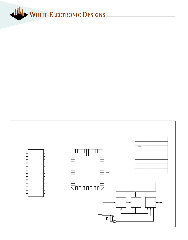
PIN DESCRIPTION
I/O
0-7
Data Inputs/Outputs
A
0-16
Address Inputs
WE
Write Enable
CS
1
, CS
2
Chip Selects
OE
Output Enable
V
CC
Power (+5V
±
10%)
V
SS
Ground
NC
Not Connected
BLOCK DIAGRAM
Memory Array
Address
Buffer
Address
Decoder
I/O
Circuits
A
ÿ-16
I/O
ÿ-7
WE
OE
CS
1
CS
2
FIG. 1
PIN CONFIGURATION
The EDI88130CS is a high speed, high performance, 128Kx8 bits
monolithic Static RAM.
An additional chip enable line provides system memory security
during power down in non-battery backed up systems and memory
banking in high speed battery backed systems where large mul-
tiple pages of memory are required.
The EDI88130CS has eight bi-directional input-output lines to
provide simultaneous access to all bits in a word.
A low power version, EDI88130LPS, offers a 2V data retention
function for battery back-up applications.
Military product is available compliant to MIL-PRF-38535.
*15ns access time is advanced information, contact factory for availability.
32 DIP
32 SOJ
32 CLCC
32 FLATPACK
TOP VIEW
32
31
30
29
28
27
26
25
24
23
22
21
20
19
18
17
1
2
3
4
5
6
7
8
9
10
11
12
13
14
15
16
V
CC
A15
CS2
WE
A13
A8
A9
A11
OE
A10
CS1
I/O7
I/O6
I/O5
I/O4
I/O3
NC
A16
A14
A12
A7
A6
A5
A4
A3
A2
A1
Aÿ
I/Oÿ
I/O1
I/O2
V
SS
32 QUAD LCC
TOP VIEW
5
6
7
8
9
10
11
12
13
29
28
27
26
25
24
23
22
21
4
3
2
1
32
31
30
14
15
16
17
18
19
20
A
7
A
6
A
5
A
4
A
3
A
2
A
1
A
0
I/O
0
I/O
1
I/O
2
V
SS
I/O
3
I/O
4
I/O
5
I/O
6
WE
A
13
A
8
A
9
A
11
OE
A
10
CS
1
I/O
7
A
12
A
14
A
16
NC
V
CC
A
15
CS
2
2
White Electronic Designs Corporation ∑ (602) 437-1520 ∑ www.whiteedc.com
EDI88130CS
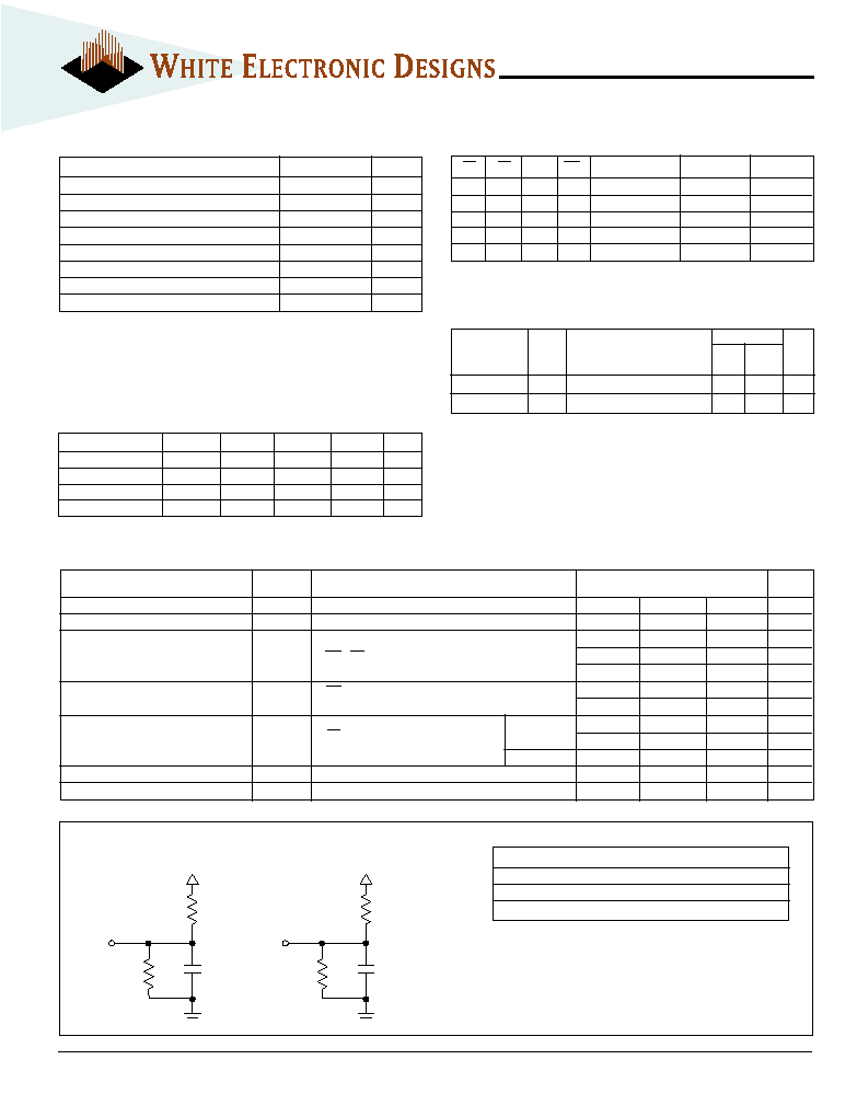
ABSOLUTE MAXIMUM RATINGS
Parameter
Unit
Voltage on any pin relative to Vss
-0.2 to 7.0
V
Operating Temperature T
A
(Ambient)
Industrial
-40 to +85
∞
C
Military
-55 to +125
∞
C
Storage Temperature, Ceramic
-65 to +150
∞
C
Power Dissipation
1.7
W
Output Current
40
mA
Junction Temperature, T
J
175
∞
C
RECOMMENDED OPERATING CONDITIONS
Parameter
Symbol
Min
Typ
Max
Unit
Supply Voltage
V
CC
4.5
5.0
5.5
V
Supply Voltage
V
SS
0
0
0
V
Input High Voltage
V
IH
2.2
--
Vcc +0.5
V
Input Low Voltage
V
IL
-0.5
--
+0.8
V
Parameter
Symbol
Condition
Max
Unit
LCC
Address Lines
C
I
V
IN
= Vcc or Vss, f = 1.0MHz
6
12
pF
Data Lines
C
O
V
OUT
= Vcc or Vss, f = 1.0MHz
8
14
pF
These parameters are sampled, not 100% tested.
CAPACITANCE
(T
A
= +25
∞
C)
TRUTH TABLE
OE
CS
1
CS
2
WE
Mode
Output
Power
X
H
X
X
Standby
High Z
Icc
2
, Icc
3
X
X
L
X
Standby
High Z
Icc
2
, Icc
3
H
L
H
H
Output Deselect
High Z
Icc
1
L
L
H
H
Read
Data Out
Icc
1
X
L
H
L
Write
Data In
Icc
1
NOTE:
Stress greater than those listed under "Absolute Maximum Ratings" may cause
permanent damage to the device. This is a stress rating only and functional
operation of the device at these or any other conditions greater than those indi-
cated in the operational sections of this specification is not implied. Exposure to
absolute maximum rating conditions for extended periods may affect reliability.
Input Pulse Levels
V
SS
to 3.0V
Input Rise and Fall Times
3ns
Input and Output Timing Levels
1.5V
Output Load
Figure 1
NOTE: For t
EHQZ
, t
GHQZ
and t
WLQZ
, CL = 5pF Figure 2)
30pF
480
Vcc
Q
Figure 1
Figure 2
255
5pF
480
Vcc
Q
255
AC TEST CONDITIONS
Parameter
Symbol
Conditions
Units
Min
Typ
Max
Input Leakage Current
I
LI
V
IN
= 0V to V
CC
--
--
±
5
µ
A
Output Leakage Current
I
LO
V
I/O
= 0V to V
CC
--
--
±
10
µ
A
(15-17ns)
--
300
mA
Operating Power Supply Current
I
CC1
WE, CS
1
= V
IL
, I
I/O
= 0mA, CS
2
= V
IH
(20ns)
--
225
mA
(25-55ns)
--
200
mA
Standby (TTL) Power Supply Current
I
CC2
CS
1
V
IH
and/or CS
2
V
IL
,
(17-55ns)
--
25
mA
V
IN
V
IH
or
V
IL
(15ns)
--
60
mA
CS
1
V
CC
-0.2V and/or CS
2
0.2V
CS (17-55ns)
--
3
10
mA
Full Standby Power Supply Current
I
CC3
CS (15ns)
--
--
15
mA
V
IN
Vcc -0.2V or V
IN
0.2V
LPS
--
--
5
mA
Output Low Voltage
V
OL
I
OL
= 8.0mA
--
--
0.4
V
Output High Voltage
V
OH
I
OH
= -4.0mA
2.4
--
--
V
DC CHARACTERISTICS
(V
CC
= 5V, T
A
= -55
∞
C to +125
∞
C)
CSOJ,DIP,
Flatpack

3
White Electronic Designs Corporation ∑ (602) 437-1520 ∑ www.whiteedc.com
EDI88130CS
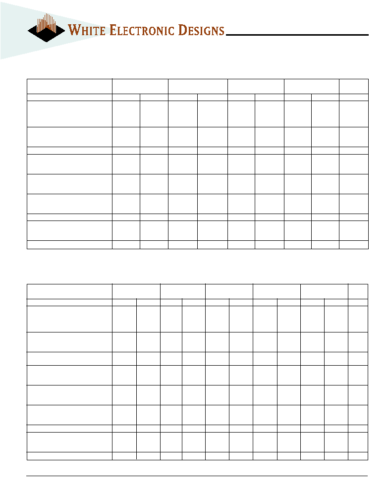
AC CHARACTERISTICS ≠ READ CYCLE (15 to 20ns)
(V
CC
= 5.0V, V
SS
= 0V, T
A
= -55
∞
C to +125
∞
C)
Symbol
15ns*
17ns
20ns
Parameter
JEDEC
Alt.
Min
Max
Min
Max
Min
Max
Units
Read Cycle Time
t
AVAV
t
RC
15
17
20
ns
Address Access Time
t
AVQV
t
AA
15
17
20
ns
Chip Enable Access Time
t
E1LQV
t
ACS
15
17
20
ns
t
E2HQV
t
ACS
15
17
20
ns
Chip Enable to Output in Low Z (1)
t
E1LQX
t
CLZ
5
5
5
ns
t
E2HQX
t
CLZ
5
5
5
ns
Chip Disable to Output in Low Z (1)
t
E1HQZ
t
CHZ
6
7
8
ns
t
E2LQZ
t
CHZ
6
7
8
ns
Output Hold from Address Change
t
AVQX
t
OH
3
3
3
ns
Output Enable to Output Valid
t
GLQV
t
OE
6
6
7
ns
Output Enable to Output in Low Z (1)
t
GLQX
t
OLZ
0
0
0
ns
Output Disable to Output in High Z(1)
t
GHQZ
t
OHZ
5
6
8
ns
Chip Enable to Power Up (1)
t
E1LICCH
t
PU
0
0
0
ns
t
E2HICCH
t
PU
0
0
0
ns
Chip Enable to Power Down (1)
t
E1HICCL
t
PD
15
17
20
ns
t
E2LICCL
t
PD
15
17
20
ns
1. This parameter is guaranteed by design but not tested.
* 15ns access time is advanced information, contact factory for availability.
AC CHARACTERISTICS ≠ READ CYCLE (25 to 55ns)
(V
CC
= 5.0V, V
SS
= 0V, T
A
= -55
∞
C to +125
∞
C)
Symbol
25ns
35ns
45ns
55ns
Parameter
JEDEC
Alt.
Min
Max
Min
Max
Min
Max
Min
Max
Units
Read Cycle Time
t
AVAV
t
RC
25
35
45
55
ns
Address Access Time
t
AVQV
t
AA
25
35
45
55
ns
Chip Enable Access Time
t
E1LQV
t
ACS
25
35
45
55
ns
Chip Enable Access Time
t
E2HQV
t
ACS
25
35
45
55
ns
Chip Enable to Output in Low Z (1)
t
E1LQX
t
CLZ
5
5
5
5
ns
t
E2HQX
t
CLZ
5
5
5
5
ns
Chip Disable to Output in Low Z (1)
t
E1HQZ
t
CHZ
10
15
20
20
ns
t
E2LQZ
t
CHZ
10
15
20
20
ns
Output Hold from Address Change
t
AVQX
t
OH
0
0
0
0
ns
Output Enable to Output Valid
t
GLQV
t
OE
10
15
20
25
ns
Output Enable to Output in Low Z (1)
t
GLQX
t
OLZ
0
0
0
0
ns
Output Disable to Output in High Z(1)
t
GHQZ
t
OHZ
10
15
20
20
ns
Chip Enable to Power Up (1)
t
E1LICCH
t
PU
0
0
0
0
ns
t
E2HICCH
t
PU
0
0
0
0
ns
Chip Enable to Power Down (1)
t
E1HICCL
t
PD
25
35
45
55
ns
t
E2LICCL
t
PD
25
35
45
55
ns
1. This parameter is guaranteed by design but not tested.
4
White Electronic Designs Corporation ∑ (602) 437-1520 ∑ www.whiteedc.com
EDI88130CS
AC CHARACTERISTICS ≠ WRITE CYCLE (15 to 20ns)
(V
CC
= 5.0V, V
SS
= 0V, T
A
= 0
∞
C to +70
∞
C)
Symbol
15ns*
17ns
20ns
Parameter
JEDEC
Alt.
Min
Max
Min
Max
Min
Max
Units
Write Cycle Time
t
AVAV
t
WC
15
17
20
ns
Chip Enable to End of Write
t
E1LWH
t
CW
12
13
15
ns
t
E1LE1H
t
CW
12
13
15
ns
t
E2HWH
t
CW
12
13
15
ns
t
E2HE2L
t
CW
12
13
15
ns
Address Setup Time
t
AVWL
t
AS
0
0
0
ns
t
AVE1L
t
AS
0
0
0
ns
t
AVE2H
t
AS
0
0
0
ns
Address Valid to End of Write
t
AVWH
t
AW
12
13
15
ns
Write Pulse Width
t
WLWH
t
WP
12
13
15
ns
t
WLE1H
t
WP
12
13
15
ns
t
WLE2L
t
WP
12
13
15
ns
Write Recovery Time
t
WHAX
t
WR
0
0
0
ns
t
E1HAX
t
WR
0
0
0
ns
t
E2LAX
t
WR
0
0
0
ns
Data Hold Time
t
WHDX
t
DH
0
0
0
ns
t
E1HDX
t
DH
0
0
0
ns
t
E2LDX
t
DH
0
0
0
ns
Write to Output in High Z (1)
t
WLQZ
t
WHZ
0
7
0
8
0
8
ns
Data to Write Time
t
DVWH
t
DW
7
8
10
ns
t
DVE1H
t
DW
7
8
10
ns
t
DVE2L
t
DW
7
8
10
ns
Output Active from End of Write (1)
t
WHQX
t
WLZ
3
3
3
ns
1. This parameter is guaranteed by design but not tested.
AC CHARACTERISTICS ≠ WRITE CYCLE (25 to 55ns)
(V
CC
= 5.0V, V
SS
= 0V, T
A
= 0
∞
C to +70
∞
C)
Symbol
25ns
35ns
45ns
55ns
Parameter
JEDEC
Alt.
Min
Max
Min
Max
Min
Max
Min
Max
Units
Write Cycle Time
t
AVAV
t
WC
25
35
45
55
ns
Chip Enable to End of Write
t
E1LWH
t
CW
20
25
35
45
ns
t
E1LE1H
t
CW
16
20
25
40
ns
t
E2HWH
t
CW
16
20
25
40
ns
t
E2HE2L
t
CW
16
20
25
40
ns
Address Setup Time
t
AVWL
t
AS
0
0
0
0
ns
t
AVE1L
t
AS
0
0
0
0
ns
t
AVE2H
t
AS
0
0
0
0
ns
Address Valid to End of Write
t
AVWH
t
AW
20
25
35
45
ns
t
AVEH
t
AW
20
25
35
45
ns
Write Pulse Width
t
WLWH
t
WP
20
30
30
35
ns
t
WLE1H
t
WP
20
30
30
35
ns
t
WLE2L
t
WP
20
30
30
35
ns
Write Recovery Time
t
WHAX
t
WR
0
0
5
5
ns
t
E1HAX
t
WR
0
0
5
5
ns
t
E2LAX
t
WR
0
0
5
5
ns
Data Hold Time
t
WHDX
t
DH
0
0
0
0
ns
t
E1HDX
t
DH
0
0
0
0
ns
t
E2LDX
t
DH
0
0
0
0
ns
Write to Output in High Z (1)
t
WLQZ
t
WHZ
0
10
0
13
0
15
0
20
ns
Data to Write Time
t
DVWH
t
DW
15
20
20
25
ns
t
DVE1H
t
DW
15
20
20
25
ns
t
DVE2L
t
DW
15
20
20
25
ns
Output Active from End of Write (1)
t
WHQX
t
WLZ
3
3
3
3
ns
1. This parameter is guaranteed by design but not tested.

5
White Electronic Designs Corporation ∑ (602) 437-1520 ∑ www.whiteedc.com
EDI88130CS
ADDRESS
DATA I/O
READ CYCLE 1 (WE HIGH; OE, CS LOW)
t
AVQX
t
AVQV
t
AVAV
DATA 2
ADDRESS 1
ADDRESS 2
DATA 1
READ CYCLE 2 (CS
1
AND/OR CS
2
CONTROLLED, WE HIGH)
ADDRESS
DATA I/O
t
AVQV
t
E1LQV
t
GLQV
t
E1LQX
t
GLQX
t
AVAV
t
E1HQZ
t
GHQZ
OE
Icc
CS
1
t
E1LICCH
t
E1HICCL
CS
2
t
E2HICCH
t
E2LICCL
t
E2HQV
t
E2HQX
FIG. 2
TIMING WAVEFORM - READ CYCLES
FIG. 3
WRITE CYCLE 1
WS32K32-XHX
FIG. 4
WRITE CYCLES 2
ADDRESS
DATA IN
WRITE CYCLE 1 - LATE WRITE, WE CONTROLLED
t
AVWH
t
WLWH
t
WHAX
t
E2HWH
t
DVWH
t
WLQZ
t
WHQX
t
AVWL
t
WHDX
t
AVAV
t
E1LWH
CS
1
DATA OUT
WE
CS
2
ADDRESS
DATA I/O
WRITE CYCLE 2 - EARLY WRITE, CS
1
CONTROLLED
t
E1LE1H
t
E1HAX
t
DVE1H
t
E1HDX
t
AVAV
CS
1
WE
CS
2
t
AVE1L
ADDRESS
DATA I/O
WRITE CYCLE 3 - EARLY WRITE, CS
2
CONTROLLED
t
E2HE2L
t
E2LAX
t
DVE2L
t
E2LDX
t
AVAV
CS
1
WE
CS
2
t
AVE2H
WRITE CYCLES 3