
1
White Electronic Designs Corporation ∑ (602) 437-1520 ∑ www.whiteedc.com
HI-RELIABILITY PRODUCT
EDI88257C
256Kx8 Monolithic SRAM
FEATURES
s 256Kx8 CMOS Static
s Random Access Memory
∑ Access Times of 70, 85, 100ns
∑ Data Retention Function (LP Versions)
∑ TTL Compatible Inputs and Outputs
∑ Fully Static, No Clocks
s JEDEC Approved Pinout
∑ 32 pin Ceramic DIP, 0.6 mils wide (Package 9)
s Single +5V (
±
10%) Supply Operation
September 1999 Rev. 2
PIN DESCRIPTION
A
0-17
Address Inputs
W
Write Enable
E
Chip Enable
G
Output Enable
DQ
0-7
Data Inputs/Outputs
V
CC
Power (+5V
±
10%)
V
SS
Ground
NC
Not Connected
BLOCK DIAGRAM
FIG. 1
PIN CONFIGURATION
The EDI88257C is a 2 Megabit 256Kx8 bit Monolithic CMOS Static
RAM.
The 32 pin DIP pinout adheres to the JEDEC standard for the two
megabit device, and is a pin replacement for the 256Kx8 module,
EDI88257C. The device is upgradeable to the 512Kx8 SRAM, the
EDI88512C. Pin 1 becomes the higher order address.
A Low Power version, EDI88257LP, offers a data retention func-
tion for battery back-up opperation. Military product is available
compliant to Appendix A of MIL-PRF-38535.
32 DIP
TOP VIEW
32
31
30
29
28
27
26
25
24
23
22
21
20
19
18
17
1
2
3
4
5
6
7
8
9
10
11
12
13
14
15
16
V
CC
A
15
A
17
W
A
13
A
8
A
9
A
11
G
A
10
E
DQ
7
DQ
6
DQ
5
DQ
4
DQ
3
NC
A
16
A
14
A
12
A
7
A
6
A
5
A
4
A
3
A
2
A
1
A
ÿ
DQ
ÿ
DQ
1
DQ
2
V
SS
Memory Array
Address
Buffer
Address
Decoder
I/O
Circuits
A
ÿ-17
DQ
ÿ-7
W
E
G

2
White Electronic Designs Corporation ∑ (602) 437-1520 ∑ www.whiteedc.com
EDI88257C
ABSOLUTE MAXIMUM RATINGS
Parameter
Unit
Voltage on any pin relative to Vss
-0.5 to 7.0
V
Operating Temperature T
A
(Ambient)
Industrial
-40 to +85
∞
C
Military
-55 to +125
∞
C
Storage Temperature, Ceramic
-65 to +150
∞
C
Power Dissipation
1
W
Output Current
20
mA
Junction Temperature, T
J
175
∞
C
RECOMMENDED OPERATING CONDITIONS
Parameter
Symbol
Min
Typ
Max
Unit
Supply Voltage
V
CC
4.5
5.0
5.5
V
Supply Voltage
V
SS
0
0
0
V
Input High Voltage
V
IH
2.2
--
Vcc +0.5
V
Input Low Voltage
V
IL
-0.3
--
+0.8
V
Parameter
Symbol
Condition
Max
Unit
Address Lines
C
I
V
IN
= Vcc or Vss, f = 1.0MHz
30
pF
Data Lines
C
D/Q
V
OUT
= Vcc or Vss, f = 1.0MHz
14
pF
These parameters are sampled, not 100% tested.
CAPACITANCE
NOTE:
Stress greater than those listed under "Absolute Maximum Ratings" may cause
permanent damage to the device. This is a stress rating only and functional
operation of the device at these or any other conditions greater than those indi-
cated in the operational sections of this specification is not implied. Exposure to
absolute maximum rating conditions for extended periods may affect reliability.
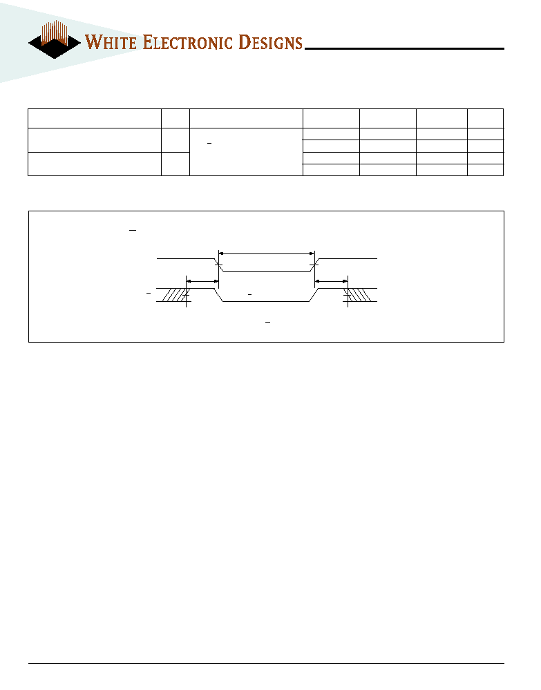
Input Pulse Levels
V
SS
to 3.0V
Input Rise and Fall Times
5ns
Input and Output Timing Levels
1.5V
Output Load
Figure 1
NOTE: For t
EHQZ
, t
GHQZ
and t
WLQZ
, CL = 5pF Figure 2)
30pF
480
Vcc
Q
Figure 1
Figure 2
255
5pF
480
Vcc
Q
255
AC TEST CONDITIONS
Parameter
Symbol
Conditions
Units
Min
Typ
Max
Input Leakage Current
I
LI
V
IN
= 0V to V
CC
--
--
±
10
µ
A
Output Leakage Current
I
LO
V
I/O
= 0V to V
CC
--
--
±
10
µ
A
Operating Power Supply Current
I
CC1
W, E = V
IL
, I
I/O
= 0mA, Min Cycle
(70-100ns)
--
45
75
mA
Standby (TTL) Power Supply Current
I
CC2
E
V
IH
, V
IN
V
IL
, V
IN
V
IH
--
3
10
mA
E
V
CC
-0.2V
C
--
--
5
mA
Full Standby Power Supply Current
I
CC3
V
IN
Vcc -0.2V or V
IN
0.2V
LP
--
--
1
mA
Output Low Voltage
V
OL
I
OL
= 2.1mA
--
--
0.4
V
Output High Voltage
V
OH
I
OH
= -1.0mA
2.4
--
--
V
DC CHARACTERISTICS
(V
CC
= 5V, T
A
= +25
∞
C)
TRUTH TABLE
G
E
W
Mode
Output
Power
X
H
X
Standby
High Z
Icc
2
, Icc
3
H
L
H
Output Deselect
High Z
Icc
1
L
L
H
Read
Data Out
Icc
1
X
L
L
Write
Data In
Icc
1

3
White Electronic Designs Corporation ∑ (602) 437-1520 ∑ www.whiteedc.com
EDI88257C
AC CHARACTERISTICS ≠ READ CYCLE
(V
CC
= 5.0V, V
SS
= 0V, T
A
= -55
∞
C to +125
∞
C))
Symbol
70ns
85ns
100ns
Parameter
JEDEC
Alt.
Min
Max
Min
Max
Min
Max
Units
Read Cycle Time
t
AVAV
t
RC
70
85
100
ns
Address Access Time
t
AVQV
t
AA
70
85
100
ns
Chip Select Access Time
t
ELQV
t
ACS
70
85
100
ns
Chip Select to Output in Low Z (1)
t
ELQX
t
CLZ
10
10
10
ns
Chip Disable to Output in High Z (1)
t
EHQZ
t
CHZ
25
30
30
ns
Output Hold from Address Change
t
AVQX
t
OH
10
10
10
ns
Output Enable to Output Valid
t
GLQV
t
OE
35
45
50
ns
Output Enable to Output in Low Z (1)
t
GLQX
t
OLZ
5
5
5
ns
Output Disable to Output in High Z (1)
t
GHQZ
t
OHZ
0
25
0
30
0
30
ns
1. This parameter is guaranteed by design but not tested.
AC CHARACTERISTICS ≠ WRITE CYCLE
(V
CC
= 5.0V, V
SS
= 0V, T
A
= -55
∞
C to +125
∞
C)
Symbol
70ns
85ns
100ns
Parameter
JEDEC
Alt.
Min
Max
Min
Max
Min
Max
Units
Write Cycle Time
t
AVAV
t
WC
70
85
100
ns
Chip Select to End of Write
t
ELWH
t
CW
60
70
80
ns
t
ELEH
t
CW
60
70
80
ns
Address Setup Time
t
AVWL
t
AS
0
0
0
ns
t
AVEL
t
AS
0
0
0
ns
Address Valid to End of Write
t
AVWH
t
AW
65
70
80
ns
t
AVEH
t
AW
65
70
80
ns
Write Pulse Width
t
WLWH
t
WP
50
55
60
ns
t
WLEH
t
WP
50
55
60
ns
Write Recovery Time
t
WHAX
t
WR
0
0
0
ns
t
EHAX
t
WR
0
0
0
ns
Data Hold Time
t
WHDX
t
DH
0
0
0
ns
t
EHDX
t
DH
0
0
0
ns
Write to Output in High Z (1)
t
WLQZ
t
WHZ
0
25
0
30
0
30
ns
Data to Write Time
t
DVWH
t
DW
40
40
40
ns
t
DVEH
t
DW
30
35
40
ns
Output Active from End of Write (1)
t
WHQX
t
WLZ
5
5
5
ns
1. This parameter is guaranteed by design but not tested.

4
White Electronic Designs Corporation ∑ (602) 437-1520 ∑ www.whiteedc.com
EDI88257C
A
Q
READ CYCLE 1 (W HIGH; G, E LOW)
t
AVQX
t
AVQV
t
AVAV
DATA 2
ADDRESS 1
ADDRESS 2
DATA 1
A
Q
READ CYCLE 2 (W HIGH)
t
AVQV
t
ELQV
t
GLQV
t
ELQX
t
GLQX
t
AVAV
t
EHQZ
t
GHQZ
G
E
WS32K32-XHX
FIG. 2
TIMING WAVEFORM - READ CYCLE
FIG. 4
WRITE CYCLE - E CONTROLLED
FIG. 3
WRITE CYCLE - W CONTROLLED
A
D
WRITE CYCLE 2, E CONTROLLED
t
AVEH
t
ELEH
t
EHAX
t
DVEH
t
EHDX
t
AVAV
DATA VALID
HIGH Z
W
t
WLEH
E
Q
t
AVEL
A
D
WRITE CYCLE 1, W CONTROLLED
t
AVWH
t
ELWH
t
WHAX
t
WLWH
t
DVWH
t
WLQZ
t
WHQX
t
AVWL
t
WHDX
t
AVAV
DATA VALID
HIGH Z
W
E
Q
5
White Electronic Designs Corporation ∑ (602) 437-1520 ∑ www.whiteedc.com
EDI88257C
Characteristic
Sym
Conditions
Min
Typ
Max
Units
Low Power Version only
Data Retention Voltage
V
DD
V
DD
= 2.0V
2
≠
≠
V
Data Retention Quiescent Current
I
CCDR
E
V
DD
-0.2V
≠
≠
185
µ
A
Chip Disable to Data Retention Time
T
CDR
V
IN
V
DD
-0.2V
0
≠
≠
ns
Operation Recovery Time
T
R
or V
IN
0.2V
T
AVAV
≠
≠
ns
DATA RETENTION CHARACTERISTICS (EDI88257LP ONLY)
(T
A
= -55
∞
C to +125
∞
C)
WS32K32-XHX
FIG. 5
DATA RETENTION - E CONTROLLED
DATA RETENTION, E CONTROLLED
Data Retention Mode
t
R
Vcc
E
t
CDR
E = V
DD
-0.2V
V
DD
4.5V
4.5V

6
White Electronic Designs Corporation ∑ (602) 437-1520 ∑ www.whiteedc.com
EDI88257C
PACKAGE 9:
32 PIN SIDEBRAZED CERAMIC DIP (600mils wide)
ALL DIMENSIONS ARE IN INCHES
Pin 1 Indicator
0.020
0.016
0.175
0.125
0.100
TYP
15 x 0.100 = 1.500
0.155
0.115
1.616
1.584
0.061
0.017
0.600
NOM
0.060
0.040
0.620
0.600
ORDERING INFORMATION
WHITE ELECTRONIC DESIGNS
SRAM
ORGANIZATION, 256Kx8
TECHNOLOGY:
C = CMOS Standard Power
LP = Low Power
ACCESS TIME (ns)
PACKAGE TYPE:
C = 32 lead Sidebrazed DIP, 600 mil (Package 9)
DEVICE GRADE:
B = MIL-STD-883 Compliant
M = Military Screened
-55
∞
C to +125
∞
C
I = Industrial
-40
∞
C to +85
∞
C
C = Commercial
0
∞
C to +70
∞
C
EDI 8 8 257 C X X X