1
White Electronic Designs Corporation ∑ (602) 437-1520 ∑ www.whiteedc.com
HI-RELIABILITY PRODUCT
EDI88257CA
256Kx8 Monolithic SRAM
FEATURES
s Access Times of 20, 25, 35, 45, 55ns
s Data Retention Function (LPA Versions)
s TTL Compatible Inputs and Outputs
s Fully Static, No Clocks
s Organized as 256Kx8
s Commercial, Industrial and Military Temperature Ranges
s JEDEC Approved Evolutionary Pinout
∑ 32 pin Ceramic DIP, 0.6 mils wide (Package 9)
s Single +5V (
±
10%) Supply Operation
May 2000 Rev. 2
PIN DESCRIPTION
I/O
0-7
Data Inputs/Outputs
A
0-17
Address Inputs
WE
Write Enable
CS
Chip Selects
OE
Output Enable
V
CC
Power (+5V
±
10%)
V
SS
Ground
NC
Not Connected
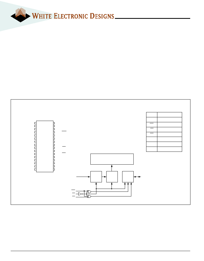
BLOCK DIAGRAM
FIG. 1
PIN CONFIGURATION
The EDI88257CA is a 2 Megabit 256Kx8 bit Monolithic CMOS
Static RAM.
The 32 pin DIP pinout adheres to the JEDEC evolutionary standard
for the two megabit device. The device is upgradeable to the
512Kx8 SRAM, the EDI88512CA. Pin 1 becomes the higher order
address.
A Low Power version, EDI88257LPA, offers a data retention
function for battery back-up opperation. Military product is avail-
able compliant to Appendix A of MIL-PRF-38535.
32 DIP
TOP VIEW
32
31
30
29
28
27
26
25
24
23
22
21
20
19
18
17
1
2
3
4
5
6
7
8
9
10
11
12
13
14
15
16
V
CC
A15
A17
WE
A13
A8
A9
A11
OE
A10
CS
I/O7
I/O6
I/O5
I/O4
I/O3
NC
A16
A14
A12
A7
A6
A5
A4
A3
A2
A1
Aÿ
I/Oÿ
I/O1
I/O2
V
SS
Memory Array
Address
Buffer
Address
Decoder
I/O
Circuits
A
ÿ-17
I/O
ÿ-7
WE
CS
OE
2
White Electronic Designs Corporation ∑ (602) 437-1520 ∑ www.whiteedc.com
EDI88257CA
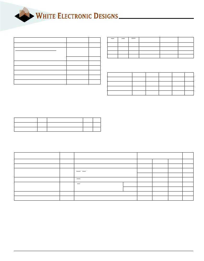
ABSOLUTE MAXIMUM RATINGS
Parameter
Unit
Voltage on any pin relative to Vss
-0.5 to 7.0
V
Operating Temperature T
A
(Ambient)
Industrial
-40 to +85
∞
C
Military
-55 to +125
∞
C
Storage Temperature, Ceramic
-65 to +150
∞
C
Power Dissipation
1.5
W
Output Current
20
mA
Junction Temperature, T
J
175
∞
C
RECOMMENDED OPERATING CONDITIONS
Parameter
Symbol
Min
Typ
Max
Unit
Supply Voltage
V
CC
4.5
5.0
5.5
V
Supply Voltage
V
SS
0
0
0
V
Input High Voltage
V
IH
2.2
--
Vcc +0.5
V
Input Low Voltage
V
IL
-0.3
--
+0.8
V
Parameter
Symbol
Condition
Max
Unit
Address Lines
C
I
V
IN
= Vcc or Vss, f = 1.0MHz
12
pF
Input/Output Lines
C
O
V
OUT
= Vcc or Vss, f = 1.0MHz
14
pF
These parameters are sampled, not 100% tested.
CAPACITANCE
(T
A
= +25
∞
C)
NOTE:
Stress greater than those listed under "Absolute Maximum Ratings" may cause
permanent damage to the device. This is a stress rating only and functional
operation of the device at these or any other conditions greater than those indi-
cated in the operational sections of this specification is not implied. Exposure to
absolute maximum rating conditions for extended periods may affect reliability.
Parameter
Symbol
Conditions
Units
Min
Typ
Max
Input Leakage Current
I
LI
V
IN
= 0V to V
CC
-10
--
+10
µ
A
Output Leakage Current
I
LO
V
I/O
= 0V to V
CC
-10
--
+10
µ
A
Operating Power Supply Current
I
CC1
WE, CS = V
IL
, I
I/O
= 0mA, Min Cycle
(20-25ns)
--
225
mA
(35-55ns)
--
200
mA
Standby (TTL) Power Supply Current
I
CC2
CS
V
IH
, V
IN
V
IL
, V
IN
V
IH
--
60
mA
CS
V
CC
-0.2V
CA
--
--
25
mA
Full Standby Power Supply Current
I
CC3
V
IN
Vcc -0.2V or V
IN
0.2V
LPA
--
--
20
mA
Output Low Voltage
V
OL
I
OL
= 8.0mA
--
--
0.4
V
Output High Voltage
V
OH
I
OH
= -4.0mA
2.4
--
--
V
NOTE: DC test conditions: V
IL
= 0.3V, V
IH
= Vcc -0.3V
DC CHARACTERISTICS
(V
CC
= 5V, T
A
= +25
∞
C)
TRUTH TABLE
OE
CS
WE
Mode
Output
Power
X
H
X
Standby
High Z
Icc
2
, Icc
3
H
L
H
Output Deselect
High Z
Icc
1
L
L
H
Read
Data Out
Icc
1
X
L
L
Write
Data In
Icc
1

3
White Electronic Designs Corporation ∑ (602) 437-1520 ∑ www.whiteedc.com
EDI88257CA
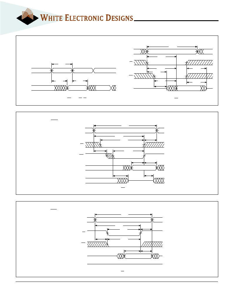
Input Pulse Levels
V
SS
to 3.0V
Input Rise and Fall Times
5ns
Input and Output Timing Levels
1.5V
Output Load
Figure 1
NOTE: For t
EHQZ
, t
GHQZ
and t
WLQZ
, CL = 5pF Figure 2)
30pF
480
Vcc
Q
Figure 1
Figure 2
255
5pF
480
Vcc
Q
255
AC TEST CONDITIONS
AC CHARACTERISTICS ≠ READ CYCLE
(V
CC
= 5.0V, V
SS
= 0V, T
A
= -55
∞
C to +125
∞
C))
Symbol
20ns
25ns
35ns
45ns
55ns
Parameter
JEDEC
Alt.
Min
Max
Min
Max
Min
Max
Min
Max
Min
Max
Units
Read Cycle Time
t
AVAV
t
RC
20
25
35
45
55
ns
Address Access Time
t
AVQV
t
AA
20
25
35
45
55
ns
Chip Select Access Time
t
ELQV
t
ACS
20
25
35
45
55
ns
Chip Select to Output in Low Z (1)
t
ELQX
t
CLZ
3
3
3
3
3
ns
Chip Disable to Output in High Z (1)
t
EHQZ
t
CHZ
0
8
0
10
0
15
0
20
0
20
ns
Output Hold from Address Change
t
AVQX
t
OH
0
0
0
0
0
ns
Output Enable to Output Valid
t
GLQV
t
OE
10
12
15
25
25
ns
Output Enable to Output in Low Z (1)
t
GLQX
t
OLZ
0
0
0
0
0
ns
Output Disable to Output in High Z (1)
t
GHQZ
t
OHZ
0
8
0
10
0
15
0
20
0
20
ns
1. This parameter is guaranteed by design but not tested.
AC CHARACTERISTICS ≠ WRITE CYCLE
(V
CC
= 5.0V, V
SS
= 0V, T
A
= -55
∞
C to +125
∞
C)
Symbol
20ns
25ns
35ns
45ns
55ns
Parameter
JEDEC
Alt.
Min
Max
Min
Max
Min
Max
Min
Max
Min
Max
Units
Write Cycle Time
t
AVAV
t
WC
20
25
35
45
45
ns
Chip Select to End of Write
t
ELWH
t
CW
15
17
25
30
30
ns
t
ELEH
t
CW
15
17
25
30
30
ns
Address Setup Time
t
AVWL
t
AS
0
0
0
0
0
ns
t
AVEL
t
AS
0
0
0
0
0
ns
Address Valid to End of Write
t
AVWH
t
AW
15
17
25
30
30
ns
t
AVEH
t
AW
15
17
25
30
30
ns
Write Pulse Width
t
WLWH
t
WP
15
17
25
30
30
ns
t
WLEH
t
WP
15
17
25
30
30
ns
Write Recovery Time
t
WHAX
t
WR
0
0
0
0
0
ns
t
EHAX
t
WR
0
0
0
0
0
ns
Data Hold Time
t
WHDX
t
DH
0
0
0
0
0
ns
t
EHDX
t
DH
0
0
0
0
0
ns
Write to Output in High Z (1)
t
WLQZ
t
WHZ
0
8
0
10
0
25
0
30
0
30
ns
Data to Write Time
t
DVWH
t
DW
10
12
20
25
25
ns
t
DVEH
t
DW
10
12
20
25
25
ns
Output Active from End of Write (1)
t
WHQX
t
WLZ
0
0
0
0
0
ns
1. This parameter is guaranteed by design but not tested.
4
White Electronic Designs Corporation ∑ (602) 437-1520 ∑ www.whiteedc.com
EDI88257CA
ADDRESS
DATA I/O
READ CYCLE 1 (WE HIGH; OE, CS LOW)
t
AVQX
t
AVQV
t
AVAV
DATA 2
ADDRESS 1
ADDRESS 2
DATA 1
ADDRESS
DATA OUT
READ CYCLE 2 (WE HIGH)
t
AVQV
t
ELQV
t
GLQV
t
ELQX
t
GLQX
t
AVAV
t
EHQZ
t
GHQZ
OE
CS
WS32K32-XHX
FIG. 2
TIMING WAVEFORM - READ CYCLE
FIG. 4
WRITE CYCLE - CS CONTROLLED
FIG. 3
WRITE CYCLE - WE CONTROLLED
ADDRESS
DATA IN
WRITE CYCLE 2, CS CONTROLLED
t
AVEH
t
ELEH
t
EHAX
t
WLEH
t
DVEH
t
EHDX
t
AVAV
DATA VALID
HIGH Z
WE
CS
DATA OUT
t
AVEL
ADDRESS
DATA IN
WRITE CYCLE 1, WE CONTROLLED
t
AVWH
t
ELWH
t
WHAX
t
WLWH
t
DVWH
t
WLQZ
t
WHQX
t
AVWL
t
WHDX
t
AVAV
DATA VALID
HIGH Z
WE
CS
DATA OUT
5
White Electronic Designs Corporation ∑ (602) 437-1520 ∑ www.whiteedc.com
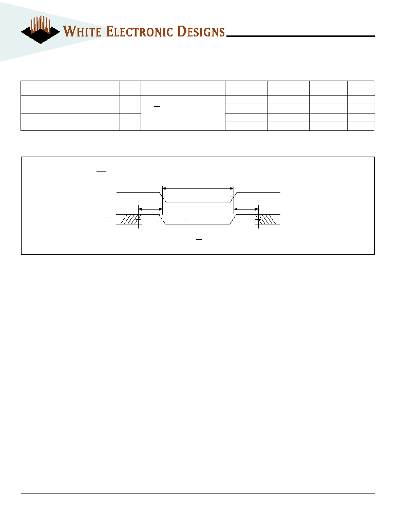
EDI88257CA
Characteristic
Sym
Conditions
Min
Typ
Max
Units
Low Power Version only
Data Retention Voltage
V
DD
V
DD
= 2.0V
2
≠
≠
V
Data Retention Quiescent Current
I
CCDR
CS
V
DD
-0.2V
≠
≠
2
mA
Chip Disable to Data Retention Time
T
CDR
V
IN
V
DD
-0.2V
0
≠
≠
ns
Operation Recovery Time
T
R
or V
IN
0.2V
T
AVAV
≠
≠
ns
DATA RETENTION CHARACTERISTICS (EDI88257LPA ONLY)
(T
A
= -55
∞
C to +125
∞
C)
WS32K32-XHX
FIG. 5
DATA RETENTION - CS CONTROLLED
DATA RETENTION, CS CONTROLLED
Data Retention Mode
t
R
Vcc
CS
t
CDR
CS = V
DD
-0.2V
V
DD
4.5V
4.5V