
EDI8F321024C
1
White Electronic Designs Corporation ∑ (602) 437-1520 ∑ www.wedc.com
White Electronic Designs
Aug. 2002
Rev. 8A
White Electronic Designs Corp. reserves the right to change products or specifications without notice.
FEATURES
1024Kx32 bit CMOS Static RAM
Access Times: 15, 20, and 25ns
Individual Byte Selects
Fully Static, No Clocks
TTL Compatible I/O
High Density Package
72 Pin ZIP, No. 175
72 lead SIMM, No. 176 (Angle)
72 lead SIMM, No. 356 (Straight)
Common Data Inputs and Outputs
Single +5V (±10%) Supply Operation
*This product is subject to change without notice.
PIN NAMES
1024Kx32 Static RAM CMOS, High Speed Module
A0-A19
Address Inputs
E0#-E3#
Chip Enables
W#
Write Enable
G#
Output Enable
DQ0-DQ31
Common Data Input/Output
V
CC
Power (+5V±10%)
V
SS
Ground
NC
No Connection
FIG. 1
PIN CONFIGURATIONS AND BLOCK DIAGRAM
DESCRIPTION
9
9
9
9
9
9
8F321024C Pin Config.
#
#
#
#
#
#
9
9
9
9
9
PD1 AND PD3 = OPEN
PD0 AND PD2 = GROUND
8F321024C Blk Dia.
W#
G#
E0#
E1#
E2#
E3#
A0-A19
DQ0-DQ3
1 Meg
X 4
DQ8-DQ11
1 Meg
X 4
DQ16-DQ19
1 Meg
X 4
DQ24-DQ27
1 Meg
X 4
DQ4-DQ7
1 Meg
X 4
DQ12-DQ15
1 Meg
X 4
DQ20-DQ23
1 Meg
X 4
DQ28-DQ31
1 Meg
X 4
The EDI8F321024C is a high speed 32 megabit Static RAM
module organized as 1024K words by 32 bits. This module
is constructed from eight 1024Kx4 Static RAMs in SOJ
packages on an epoxy laminate (FR4) board.
Four chip enables (Eÿ#-E3#) are used to independently
enable the four bytes. Reading or writing can be executed
on individual bytes or any combination of multiple bytes
through proper use of selects.
The EDI8F321024C is offered in 72 pin ZIP and 72 lead
SIMM packages, which enable 32 megabits of memory to
be placed in less than 1.3 square inches of board space.
All inputs and outputs are TTL compatible and operate from
a single 5V supply. Fully asynchronous circuitry requires
no clocks or refreshing for operation and provides equal
access and cycle times for ease of use.
Pins PD1- PD4, are used to identify module memory
density in applications where alternate modules can be
interchanged.

EDI8F321024C
2
White Electronic Designs Corporation ∑ (602) 437-1520 ∑ www.wedc.com
White Electronic Designs
Aug. 2002
Rev. 8A
White Electronic Designs Corp. reserves the right to change products or specifications without notice.
ABSOLUTE MAXIMUM RATINGS*
RECOMMENDED DC OPERATING CONDITIONS
DC
EL
ECTRICAL CHARACTERISTICS
CAPACITANCE
(f=1.0MHz, V
IN
=V
CC
or V
SS
)
TRUTH TABLE
AC TEST CONDITIONS
*Stress greater than those listed under "Absolute Maximum Ratings" may
cause permanent damage to the device. This is a stress rating only and
functional operation of the device at these or any other conditions greater
than those indicated in the operational sections of this specification is not
implied. Exposure to absolute maximum rating conditions for extended
periods may affect reliability.
(Note: For t
EHQZ
,t
GHQZ
and t
WLQZ
, CL = 5pF)
*Typical: T
A
= 25∞C, V
CC
= 5.0V
These parameters are sampled, not 100% tested.
E#
W#
G#
Mode
Output
Power
H
X
X
Standby
HIGH Z
I
CC2
/I
CC3
L
H
L
Read
D
OU
t
I
CC1
L
L
X
Write
D
IN
I
CC1
L
H
H
Output
Deselect
HIGH Z
I
CC1
Parameter
Sym
Max
Unit
Address Lines
CI
60
pF
Data Lines
CD/Q
20
pF
Chip Enable Line
CC
20
pF
Write Line
CN
60
pF
Voltage on any pin relative to V
SS
-0.5V to 7.0V
Operating Temperature T
A
(Ambient)
Commercial
Industrial
0∞C to +70∞C
-40∞C to +85∞C
Storage Temperature, Plastic
-55∞C to +125∞C
Power Dissipation
7.0 Watts
Output Current
20 mA
Input Pulse Levels
V
SS
to 3.0V
Input Rise and Fall Times
5ns
Input and Output Timing Levels
1.5V
Output Load
1TTL, CL = 30pF
Parameter
Sym
Min
Typ
Max
Units
Supply Voltage
V
CC
4.5
5.0
5.5
V
Supply Voltage
V
SS
0
0
0
V
Input High Voltage
V
IH
2.2
≠
6.0
V
Input Low Voltage
V
IL
-0.3
≠
0.8
V
Parameter
Sym
Conditions
Min
Typ
Max
Units
Operating Power Supply Current
I
CC1
W#, E# = V
IL
, II/O = 0mA, Min Cycle
1280
mA
Standby (TTL) Power Supply Current
I
CC2
E# V
IH
, V
IN
V
IL
or V
IN
V
IH
480
mA
Full Standby Power Supply Current
CMOS
I
CC3
E# V
CC
-0.2V
V
IN
V
CC
-0.2V or V
IN
0.2V
80
mA
Input Leakage Current
I
LI
V
IN
= 0V to V
CC
≠
≠
±80
µA
Output Leakage Current
I
LO
V I/O = 0V to V
CC
≠
≠
±20
µA
Output High Voltage
V
OH
I
OH
= -4.0mA
2.4
≠
≠
V
Output Low Voltage
V
OL
I
OL
= 8.0mA
≠
≠
0.4
V

EDI8F321024C
3
White Electronic Designs Corporation ∑ (602) 437-1520 ∑ www.wedc.com
White Electronic Designs
Aug. 2002
Rev. 8A
White Electronic Designs Corp. reserves the right to change products or specifications without notice.
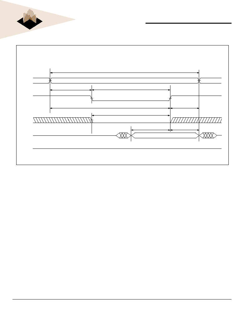
AC CHARACTERISTICS READ CYCLE
Note 1: Parameter guaranteed, but not tested.
READ CYCLE 1 - W# HIGH, G#, E# LOW
FIG.
FIG. 3
ADDRESS 1
ADDRESS 2
t
AVAV
DATA 1
DATA 2
t
AVQV
t
AVQX
A
Q
t
GHQZ
t
ELQV
t
ELQX
E#
G#
Q
t
EHQZ
A
t
AVAV
t
GLQV
t
GLQX
t
AVQV
8F8512C Rd Cyc2
Parameter
Symbol
15ns
20ns
25ns
Units
JEDEC
Alt.
Min
Max
Min
Max
Min
Max
Read Cycle Time
t
AVAV
t
RC
15
20
25
ns
Address Access Time
t
AVQV
t
AA
15
20
25
ns
Chip Enable Access
t
ELQV
t
ACS
15
20
25
ns
Chip Enable to Output in Low Z (1)
t
ELQX
t
CLZ
3
3
3
ns
Chip Disable to Output in High Z (1)
t
EHQZ
t
CHZ
7
10
12
ns
Output Hold from Address Change
t
AVQX
t
OH
3
3
3
ns
Output Enable to Output Valid
t
GLQV
t
OE
7
8
10
ns
Output Enable to Output in Low Z (1)
t
GLQX
t
OLZ
0
0
0
ns
Output Disable to Output in High Z(1)
t
GHQZ
t
OHZ
7
8
10
ns
READ CYCLE 2 - W# HIGH

EDI8F321024C
4
White Electronic Designs Corporation ∑ (602) 437-1520 ∑ www.wedc.com
White Electronic Designs
Aug. 2002
Rev. 8A
White Electronic Designs Corp. reserves the right to change products or specifications without notice.
Note 1: Parameter guaranteed, but not tested.
WRITE CYCLE 1 - W# CONTROLLED
AC CHARACTERISTICS WRITE CYCLE
FIG. 4
E#
A
t
AVAV
t
ELWH
t
AVWH
t
WLWH
t
AVWL
t
WHAX
W#
HIGH Z
DATA VALID
t
WLQZ
t
WHQX
t
DVWH
t
WHDX
Q
D
8F8512C Write Cyc1
Symbol
15ns
20ns
25ns
Parameter
JEDEC
Alt.
Min
Max
Min
Max
Min
Max
Units
Write Cycle Time
t
AVAV
t
WC
15
20
25
ns
Chip Enable to End of Write
t
ELWH
t
WLEH
t
CW
t
CW
10
10
15
15
20
20
ns
ns
Address Setup Time
t
AVWL
t
AVEL
t
AS
t
AS
0
0
0
0
0
0
ns
ns
Address Valid to End of Write
t
AVWH
t
AVEH
t
AW
t
AW
10
10
15
15
20
20
ns
ns
Write Pulse Width
t
WLWH
t
ELEH
t
WP
t
WP
12
12
15
15
20
20
ns
ns
Write Recovery Time
t
WHAX
t
EHAX
t
WR
t
WR
0
0
0
0
0
0
ns
ns
Data Hold Time
t
WHDX
t
EHDX
t
DH
t
DH
3
3
3
3
0
0
ns
ns
Write to Output in High Z (1)
t
WLQZ
t
WHZ
0
7
0
8
0
12
ns
Data to Write Time
t
DVWH
t
DVEH
t
DW
t
DW
7
7
12
12
15
15
ns
ns
Output Active from End of Write (1)
t
WHQX
t
WLZ
3
3
3
ns
EDI8F321024C
5
White Electronic Designs Corporation ∑ (602) 437-1520 ∑ www.wedc.com
White Electronic Designs
Aug. 2002
Rev. 8A
White Electronic Designs Corp. reserves the right to change products or specifications without notice.
WRITE CYCLE 2 - E# CONTROLLED
FIG. 5
A
t
AVEL
HIGH Z
t
AVAV
8F8512C Write Cyc2
t
ELEH
E#
t
AVEH
t
EHAX
W#
t
WLEH
t
EHDX
t
DVEH
Q
DATA VALID
D

EDI8F321024C
6
White Electronic Designs Corporation ∑ (602) 437-1520 ∑ www.wedc.com
White Electronic Designs
Aug. 2002
Rev. 8A
White Electronic Designs Corp. reserves the right to change products or specifications without notice.
176-8F321024C Pkg.
.400 .250
.250 TYP.
1.992
4.255 MAX.
3.984
.062 R.
.062 R.
.050
TYP.
.680
MAX.
.125
MIN.
MIN.
.360
MAX.
.225
3.750
2.045
ORDERING INFORMATION
Note: To order gold SIMM option, change "EDIF" to "EDIG".
PACKAGE DESCRIPTIONS
.360
MAX.
.100
TYP.
P1
.050
.050
3.865 MAX.
.020
.100 TYP.
.052 TYP.
.250 TYP.
.175
.125
.590
MAX.
175-8F321024C Pkg.
PACKAGE NO.175: 72 PIN ZIP
J2
J1
J4
R.#
P1
.125 DIA (2x)
164
356-8F321024C Pkg.
.400
.250
.050 TYP.
.250 TYP.
1.992
4.255 MAX.
3.984
.062 R. (2x)
.600
MAX.
.125
MIN.
.360
MAX.
3.750
2.045
ALL DIMENSIONS ARE IN INCHES
Part Number
Speed (ns)
Package No.
EDI8F321024C15MNC
15
176
EDI8F321024C20MNC
20
176
EDI8F321024C25MNC
25
176
NOT RECOMMENDED FOR NEW DESIGNS
Part Number
Speed (ns)
Package No.
EDI8F321024C15MZC
15
175
EDI8F321024C20MZC
20
175
EDI8F321024C25MZC
25
175
EDI8F321024C15MMC
15
356
EDI8F321024C20MMC
20
356
EDI8F321024C25MMC
25
356
PACKAGE NO. 176: 72 LEAD ANGLED SIMM
PACKAGE NO. 356: 72 PIN SIMM