1
White Electronic Designs Corporation ∑ (602) 437-1520 ∑ www.wedc.com
White Electronic Designs
EDI8F32259V
Oct 2002
Rev. 0A
White Electronic Designs Corp. reserves the right to change products or specifications without notice.
256Kx32 Static RAM CMOS, High Speed Module
DESCRIPTION
The EDI8F32259V is a high speed 8Mb Static RAM module
organized as 256K words by 32 bits. This module is constructed
from eight 256Kx4 Static RAMs in SOJ packages on an epoxy
laminate (FR4) board.
Four chip enables (E0#-E3#) are used to independently
enable the four bytes. Reading or writing can be executed on
individual bytes or any combination of multiple bytes through
proper use of selects.
The EDI8F32259V is offered in 72 pin ZIP/SIMM package
which enables eight megabits of memory to be placed in less
than 1.3 square inches of board space.
All inputs and outputs are t
TL
compatible and operate from a
single 3.3V supply. Fully asynchronous circuitry requires no
clocks or refreshing for operation and provides equal access
and cycle times for ease of use.
The ZIP and SIMM modules contain four P
D
(Presence Detect)
pins which are used to identify module memory density in
applications where alternate modules can be interchanged.
FEATURES
n
256Kx32 bit CMOS Static RAM
n
Access Times: 12, 15, 20, and 25ns
n
Individual Byte Selects
n
Fully Static, No Clocks
n
t
TL
Compatible I/O
n
High Density Package with JEDEC Standard Pinouts
n
72 Pin SIMM No. 175 (Angle)
n
72 Pin ZIP No. 176
n
72 Pin SIMM No. 354 (Straight)
n
Single +3.3V (±10%) Supply Operation
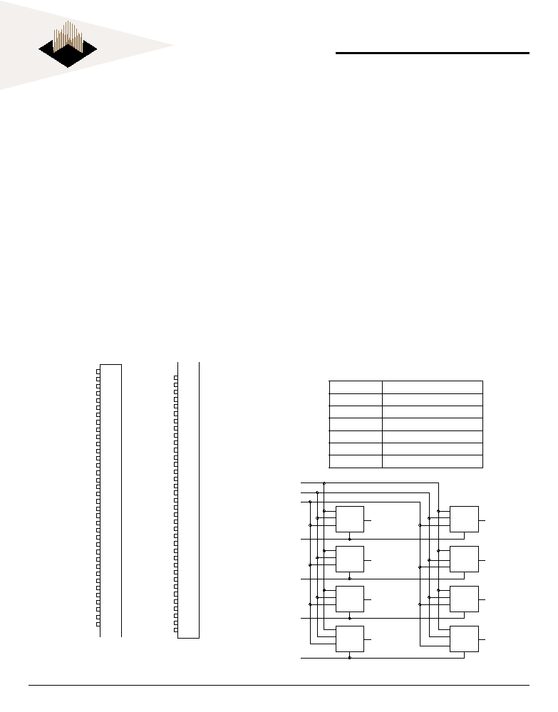
PIN NAMES
PIN CONFIGURATIONS AND BLOCK DIAGRAM
A0-A17
Address Inputs
E0#-E3#
Chip Enables
W#
Write Enables
G#
Output Enable
DQ0-DQ31
Common Data Input/Output
V
CC
Power (+5V ±10%)
V
SS
Ground
FIG. 1

2
White Electronic Designs Corporation ∑ (602) 437-1520 ∑ www.wedc.com
White Electronic Designs
EDI8F32259V
Oct 2002
Rev. 0A
White Electronic Designs Corp. reserves the right to change products or specifications without notice.
ABSOLUTE MAXIMUM RATINGS*
RECOMMENDED DC OPERATING CONDITIONS
DC ELECTRICAL CHARACTERISTICS
CAPACITANCE
(f=1.0MHz, V
IN
=V
CC
or V
SS
)
AC TEST CONDITIONS
Note: For t
EHQZ
,t
GHQZ
and t
WLQZ
, CL = 5pF)
Note: Typical: t
A
= 25∞C, V
CC
= 5.0V
TRUTH TABLE
Note: These parameters are sampled, not 100% tested.
*Stress greater than those listed under "Absolute Maximum Ratings"
may cause permanent damage to the device. This is a stress rating
only and functional operation of the device at these or any other
conditions greater than those indicated in the operational sections of
this specification is not implied. Exposure to absolute maximum rating
conditions for extended periods may affect reliability.
Voltage on any pin relative to V
SS
-0.5V to 4.6V
Operating Temperature t
A
(Ambient)
Commercial
0∞C to +70∞C
Storage Temperature, Plastic
-55∞C to +125∞C
Power Dissipation
2.5 Watt
Output Current
20 mA
Input Pulse Levels
V
SS
to 3.0V
Input Rise and Fall Times
5ns
Input and Output Timing Levels
1.5V
Output Load
1t
TL
, CL = 30pF
Parameter
Sym
Min
Typ
Max
Units
Supply Voltage
V
CC
3.0
3.3
3.6
V
Supply Voltage
V
SS
0
0
0
V
Input High Voltage
V
IH
2.2
--
V
CC
+0.3V
V
Input Low Voltage
V
IL
-0.3
--
0.8
V
Parameter
Sym
Conditions
Min
Max
12-25
Units
ns
Operating Power Supply Current
I
CC1
W#, E# = V
IL
, II/O = 0mA, Min Cycle
800
mA
Standby (t
TL
) Power Supply Current
I
CC2
E# V
IH
, V
IN
V
IL
or V
IN
V
IH
240
mA
Full Standby Power Supply Current
CMOS
I
CC3
E# V
CC
-0.2V
V
IN
V
CC
-0.2V or V
IN
0.2V
40
mA
Input Leakage Current
I
LI
V
IN
= 0V to V
CC
--
±80
µA
Output Leakage Current
I
LO
V I/O = 0V to V
CC
--
±20
µA
Output High Voltage
V
OH
I
OH
= -4.0mA
2.4
--
V
Output Low Voltage
V
OL
I
OL
= 8.0mA
--
0.4
V
E# W# G#
Mode
Output
Power
H
X
X
Standby
HIGH Z
I
CC3
L
H
L
Read
D
OUT
I
CC1
L
L
X
Write
D
IN
I
CC1
L
H
H
Output Deselect
HIGH Z
I
CC1
Parameter
Sym
Max
Unit
Address Lines
CI
60
pF
Data Lines
CD/Q
20
pF
Chip Enable Line
CC
20
pF
Write Control Line
CN
60
pF
3
White Electronic Designs Corporation ∑ (602) 437-1520 ∑ www.wedc.com
White Electronic Designs
EDI8F32259V
Oct 2002
Rev. 0A
White Electronic Designs Corp. reserves the right to change products or specifications without notice.
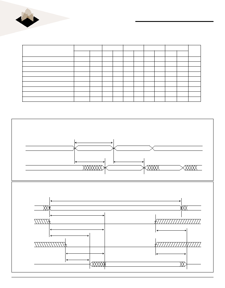
AC CHARACTERISTICS READ CYCLE
READ CYCLE 2 - W# HIGH
Note: 1. Parameter guaranteed, but not tested.
READ CYCLE 1 - W# HIGH, G#, E# LOW
FIG. 3
FIG. 2
Parameter
Symbol
12ns
15ns
20ns
25ns
Units
JEDEC
Alt.
Min
Max
Min
Max
Min
Max
Min
Max
Read Cycle Time
t
AVAV
t
RC
12
15
20
25
ns
Address Access Time
t
AVQV
t
AA
12
15
20
25
ns
Chip Enable Access
t
ELQV
t
ACS
12
15
20
25
ns
Chip Enable to Output in Low Z (1)
t
ELQX
t
CLZ
3
3
3
3
ns
Chip Disable to Output in High Z (1)
t
EHQZ
t
CHZ
6
7
9
9
ns
Output Hold from Address Change
t
AVQX
t
OH
3
3
3
3
ns
Output Enable to Output Valid
t
GLQV
t
OE
6
7
9
9
ns
Output Enable to Output in Low Z (1)
t
GLQX
t
OLZ
0
0
0
0
ns
Output Disable to Output in High Z (1)
t
GHQZ
t
OHZ
6
7
9
9
ns

4
White Electronic Designs Corporation ∑ (602) 437-1520 ∑ www.wedc.com
White Electronic Designs
EDI8F32259V
Oct 2002
Rev. 0A
White Electronic Designs Corp. reserves the right to change products or specifications without notice.
Note 1: Parameter guaranteed, but not tested.
AC CHARACTERISTICS WRITE CYCLE
Parameter
Symbol
12ns
15ns
20ns
25ns
Units
JEDEC
Alt.
Min Max Min Max Min Max Min
Max
Write Cycle Time
t
AVAV
t
WC
12
15
20
25
ns
Chip Enable to End of Write
t
ELWH
t
WLEH
t
CW
t
CW
8
8
9
9
10
10
10
10
ns
ns
Address Setup Time
t
AVWL
t
AVEL
t
AS
t
AS
0
0
0
0
0
0
0
0
ns
ns
Address Valid to End of Write
t
AVWH
t
AVEH
t
AW
t
AW
8
8
9
9
10
10
10
10
ns
ns
Write Pulse Width
t
WLWH
t
ELEH
t
WP
t
WP
8
8
9
9
10
10
10
10
ns
ns
Write Recovery Time
t
WHAX
t
EHAX
t
WR
t
WR
0
0
0
0
0
0
0
0
ns
ns
Data Hold Time
t
WHDX
t
EHDX
t
DH
t
DH
3
3
3
3
3
3
3
3
ns
ns
Write to Output in High Z (1)
t
WLQZ
t
WHZ
0
6
0
7
0
9
0
9
ns
Data to Write Time
t
DVWH
t
DVEH
t
DW
t
DW
6
6
7
7
8
8
8
8
ns
ns
Output Active from End of Write (1)
t
WHQX
t
WLZ
3
3
3
3
ns
5
White Electronic Designs Corporation ∑ (602) 437-1520 ∑ www.wedc.com
White Electronic Designs
EDI8F32259V
Oct 2002
Rev. 0A
White Electronic Designs Corp. reserves the right to change products or specifications without notice.
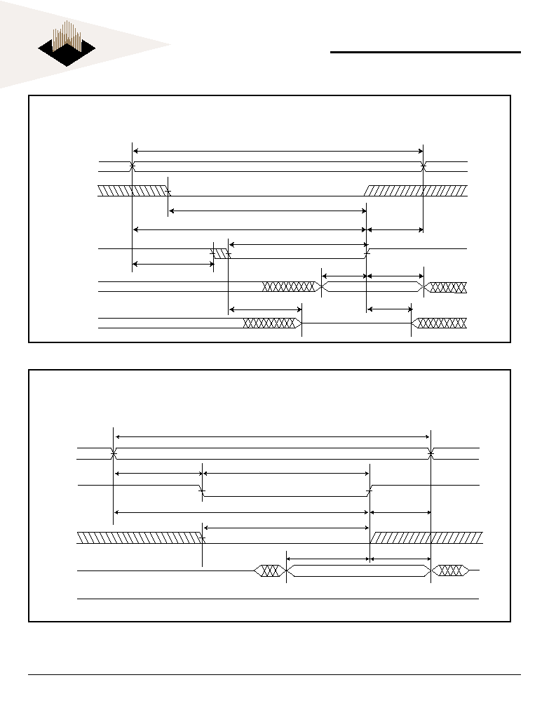
WRITE CYCLE 1 - W# CONTROLLED
WRITE CYCLE 2 - E# CONTROLLED
FIG. 4
FIG. 5

6
White Electronic Designs Corporation ∑ (602) 437-1520 ∑ www.wedc.com
White Electronic Designs
EDI8F32259V
Oct 2002
Rev. 0A
White Electronic Designs Corp. reserves the right to change products or specifications without notice.
PACKAGE DESCRIPTION
PACKAGE NO. 175: 72 PIN ZIP
NOTE: 1. For Gold SIMM change form EDI8F to EDI8G.
ORDERING INFORMATION
Part Number
Speed
(ns)
Package
No.
EDI8F32259V12MNC
12
176
EDI8F32259V15MNC
15
176
EDI8F32259V20MNC
20
176
EDI8F32259V25MNC
25
176
EDI8F32259V12MMC
12
354
EDI8F32259V15MMC
15
354
EDI8F32259V20MMC
20
354
EDI8F32259V25MMC
25
354
EDI8F32259V12MZC
12
175
EDI8F32259V15MZC
15
175
EDI8F32259V20MZC
20
175
EDI8F32259V25MZC
25
175
NOT RECOMMENDED FOR NEW DESIGNS

7
White Electronic Designs Corporation ∑ (602) 437-1520 ∑ www.wedc.com
White Electronic Designs
EDI8F32259V
Oct 2002
Rev. 0A
White Electronic Designs Corp. reserves the right to change products or specifications without notice.
PACKAGE NO. 354: 72 PIN SIMM STRAIGHT
PACKAGE NO. 176: 72 PIN ANGLED
ALL DIMENSIONS ARE IN INCHES
.360
MAX.
.225
MIN.
MIN.
.250
.052 TYP.
.250
.125
.680
MAX.
+
+
J2
J1
J4
P1
110
REV.#
4.255 MAX.
.125 DIA (2x)
.062 R.
2.045
.062 R.
3.750
1.992
.400
3.984
.360
MAX.
MIN.
.250
.052 TYP.
.250
.125
.680
MAX.
+
+
J2
J1
J4
P1
110
REV.#
4.255 MAX.
.125 DIA (2x)
.062 R.
2.045
.062 R.
3.750
1.992
.400
3.984